Intel SE7525GP2 Product Specification - Page 158
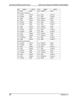
Table 77. HSBP Header Pin-out J30
 |
View all Intel SE7525GP2 manuals
Add to My Manuals
Save this manual to your list of manuals |
Page 158 highlights
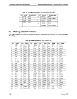
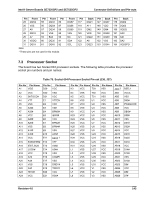
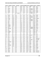
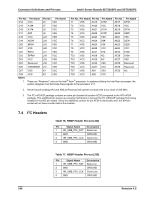
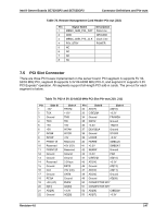
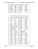
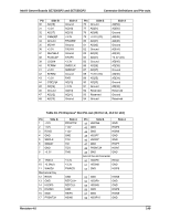
Connector Definitions and Pin-outs Intel® Server Boards SE7320SP2 and SE7525GP2 Pin No Pin Name Pin No Pin Name D14 VCC J6 VCC Pin No Pin Name Pin No Pin Name Pin No Pin Name T1 VSS AA19 D15# AE17 DP3# D15 A18# J7 VSS T2 VCC AA20 VCC AE18 VCC D16 A17# J8 VCC T3 VSS AA21 D11# AE19 DP1# D17 A9# J9 VSS T4 VCC AA22 D10# AE20 D28# D18 VCC J23 VSS T5 VSS AA23 VSS AE21 VSS D19 ADS# J24 VCC T6 VCC AA24 D6# AE22 D27# D20 BR0# J25 VSS T7 VSS AA25 D3# AE23 D22# D21 VSS J26 VCC T8 VCC AA26 VCC AE24 VCC D22 RS1# J27 VSS T9 VSS AA27 D1# AE25 D19# D23 BPRI# J28 VCC T23 VSS AA28 NC AE26 D16# D24 VCC J29 VSS T24 VCC AA29 NC AE27 VSS D25 Reserved J30 VCC T25 VSS AA30 VSS AE28 Reserved D26 VSSSENSE J31 VSS T26 VCC AA31 VCC AE29 Reserved D27 VSS K1 VCC T27 VSS AB1 VSS AE30 NC D28 Notes: 1. VSS K2 VSS T28 VCC AB2 VCC These are "Reserved " pins on the Intel® Xeon® processor. In systems utilizing the Intel Xeon processor, the system designer must terminate these signals to the processor VTT. 2. Server boards treating AA3 and AB3 as Reserved will operate correctly with a bus clock of 200 MHz. 3. The FC-mPGA2P package contains an extra pin (located at location AE30) compared to the INT-mPGA package. This additional pin serves as a keying mechanism to prevent the FC-mPGA2P package from being installed in the 603-pin socket. Since the additional contact for pin AE30 is electrically inert, the 604-pin socket will not have a solder ball at this location. 7.4 I2C Headers Table 76. HSBP Header Pin-out (J54) Pin Signal Name Description 1 HR_SMB_P5V_DAT Data Line 2 GND GROUND 3 HR_SMB_P5V_CLK Clock Line 4 GND GROUND Table 77. HSBP Header Pin-out (J30) Pin Signal Name Description 1 HR_SMB_P5V_DAT Data Line 2 GND GROUND 3 HR_SMB_P5V_CLK Clock Line 4 GND GROUND 146 Revision 4.0
-
 1
1 -
2
-
3
-
4
-
5
-
6
-
7
-
8
-
9
-
10
-
11
-
12
-
13
-
14
-
15
-
16
-
17
-
18
-
19
-
20
-
21
-
22
-
23
-
24
-
25
-
26
-
27
-
28
-
29
-
30
-
31
-
32
-
33
-
34
-
35
-
36
-
37
-
38
-
39
-
40
-
41
-
42
-
43
-
44
-
45
-
46
-
47
-
48
-
49
-
50
-
51
-
52
-
53
-
54
-
55
-
56
-
57
-
58
-
59
-
60
-
61
-
62
-
63
-
64
-
65
-
66
-
67
-
68
-
69
-
70
-
71
-
72
-
73
-
74
-
75
-
76
-
77
-
78
-
79
-
80
-
81
-
82
-
83
-
84
-
85
-
86
-
87
-
88
-
89
-
90
-
91
-
92
-
93
-
94
-
95
-
96
-
97
-
98
-
99
-
100
-
101
-
102
-
103
-
104
-
105
-
106
-
107
-
108
-
109
-
110
-
111
-
112
-
113
-
114
-
115
-
116
-
117
-
118
-
119
-
120
-
121
-
122
-
123
-
124
-
125
-
126
-
127
-
128
-
129
-
130
-
131
-
132
-
133
-
134
-
135
-
136
-
137
-
138
-
139
-
140
-
141
-
142
-
143
-
144
-
145
-
146
-
147
-
148
-
149
-
150
-
151
-
152
-
 153
153 -
 154
154 -
 155
155 -
 156
156 -
 157
157 -
 158
158 -
 159
159 -
 160
160 -
 161
161 -
 162
162 -
 163
163 -
164
-
165
-
166
-
167
-
168
-
169
-
170
-
171
-
172
-
173
-
174
-
175
-
176
-
177
-
178
-
179
-
180
-
181
-
182
-
183
-
184
 |
 |