Intel SE7525GP2 Product Specification - Page 53
Intel® Server Boards SE7320SP2 and SE7525GP2, Functional Architecture, Revision 4.0, Table 15. Super
 |
View all Intel SE7525GP2 manuals
Add to My Manuals
Save this manual to your list of manuals |
Page 53 highlights
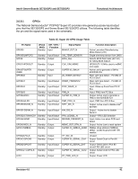
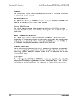
Intel® Server Boards SE7320SP2 and SE7525GP2 Functional Architecture 3.6.9.1 GPIOs The National Semiconductor* PC87427 Super I/O provides nine general-purpose input/output pins that the SE7320SP2 and Server Board SE7525GP2 utilizes. The following table identifies the pin and the signal name used in the schematic: Table 15. Super I/O GPIO Usage Table Pin Name GPIO00 (Powe Well) Standby GPIO05/LMPCIF2 GPIO6 GPIO7/HFCKOUT Standby Standby Standby GPIO27/SUPER IOSMI GPIOE40 GPIOE41 Standby Standby Standby GPIOE42 GPIOE43 GPIOE44/SCI Standby Standby Standby GPIOE45/LED GPIO50/DCDM_N Standby Standby GPIO51/DSRM_N Standby GPIO52/CTSM/XCS1 Standby GPIO54/SINM Standby GPO60/WDO_N GPO61/SMBSA Standby Standby GPO62/LFCLK GPEXC/GPIO56 Standby Standby GPEXD/GPIO57 Standby GPEXC2 / LMPCLK Standby LED1 Standby GPI / GPO / Function Input Input/Output Output Output Output Input Input/Output Input/Output Input/Output Input/Output Input/Output Input/Output Input/Output Input/Output Input/Output Output Output Output Output Input/Output Output Output Signal Name MANUF_DET_N SIO_TEMP_SENSOR BIOS_SEL CLK_10M_MBMC SUPER IO_SMI_N 2U_RISER_DETECT RISER_PRESENT2 PCIE_WAKE_N PME_N SUPER IO_PME_N PME_PCIX_N NWY_DIS_N KNI_DIS_N FRU_LEDSEL_N MROMB_PRESENT_N MBMC_RST_BTN_N SUPER IO_SMBUS_ADDR TP_SIO_45 SUPER IO_SERIAL_CLK1 SUPER IO_SERIAL_DAT SUPER IO_SERIAL_CLK2 FP_PWR_LED_N Function Description Active Low when Manufacturing Mode Detect (J35) Single wire temp sensor from LM30. Selects BIOS flash bank (A21 bit) for rolling BIOS feature. HFCKOUT- 10 MHz clock to mBMC (not used) Active Low to generate a SMI to 6300ESB ICH Riser card type detect - Pin B92 of PCI-X Slot 1. Riser card type detect - Pin B93 of PCI-X Slot 1. Input- Wake up Event from PCI-E Bus Intput- PME from PCI Bus Output- Active Low to generate a PME to the 6300ESB ICH Input- PME from PCI-X Bus Output- Active Low to disable Intel® 82570EI Output - Active low to disable Kenai-II Output - FRU LED Selection Input- Active Low when ZCR card detect Output- Active Low to reset system SMBus slave address (SMBSA) select - pulled to ground with 10K resistor. Unused Output- Serial Clock to Port 80 circuit Output- Serial data to Port 80 circuit/FRU LED circuit Output- Serial Clock to FRU LED circuit Output- Power LED Revision 4.0 41
-
 1
1 -
2
-
3
-
4
-
5
-
6
-
7
-
8
-
9
-
10
-
11
-
12
-
13
-
14
-
15
-
16
-
17
-
18
-
19
-
20
-
21
-
22
-
23
-
24
-
25
-
26
-
27
-
28
-
29
-
30
-
31
-
32
-
33
-
34
-
35
-
36
-
37
-
38
-
39
-
40
-
41
-
42
-
43
-
44
-
45
-
46
-
47
-
 48
48 -
 49
49 -
 50
50 -
 51
51 -
 52
52 -
 53
53 -
 54
54 -
 55
55 -
 56
56 -
 57
57 -
 58
58 -
59
-
60
-
61
-
62
-
63
-
64
-
65
-
66
-
67
-
68
-
69
-
70
-
71
-
72
-
73
-
74
-
75
-
76
-
77
-
78
-
79
-
80
-
81
-
82
-
83
-
84
-
85
-
86
-
87
-
88
-
89
-
90
-
91
-
92
-
93
-
94
-
95
-
96
-
97
-
98
-
99
-
100
-
101
-
102
-
103
-
104
-
105
-
106
-
107
-
108
-
109
-
110
-
111
-
112
-
113
-
114
-
115
-
116
-
117
-
118
-
119
-
120
-
121
-
122
-
123
-
124
-
125
-
126
-
127
-
128
-
129
-
130
-
131
-
132
-
133
-
134
-
135
-
136
-
137
-
138
-
139
-
140
-
141
-
142
-
143
-
144
-
145
-
146
-
147
-
148
-
149
-
150
-
151
-
152
-
153
-
154
-
155
-
156
-
157
-
158
-
159
-
160
-
161
-
162
-
163
-
164
-
165
-
166
-
167
-
168
-
169
-
170
-
171
-
172
-
173
-
174
-
175
-
176
-
177
-
178
-
179
-
180
-
181
-
182
-
183
-
184
 |
 |