Intel SE7525GP2 Product Specification - Page 64
Accessing Configuration Space
 |
View all Intel SE7525GP2 manuals
Add to My Manuals
Save this manual to your list of manuals |
Page 64 highlights
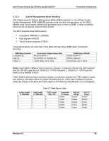
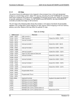
Functional Architecture Intel® Server Boards SE7320SP2 and SE7525GP2 Address (es) 03E8h - 03Efh 03F0h - 03F5h 03F6h - 03F7h 03F8h - 03FFh 0400h - 043Fh 0461h 0480h - 048Fh 04C0h - 04CFh 04D0h - 04D1h 04D4h - 04D7h 04D8h - 04DFh 04E0h - 04FFh 051Ch 0678h - 067Ah 0778h - 077Ah 07BCh - 07Beh 0CF8h 0CF9h 0CFCh Serial Port A Resource Floppy Disk Controller Primary IDE - Sec Floppy Serial Port A (primary) DMA Controller 1, Extended Mode Registers Extended NMI / Reset Control DMA High Page Register DMA Controller 2, High Base Register Interrupt Controllers 1 and 2 Control Register DMA Controller 2, Extended Mode Register Reserved DMA Channel Stop Registers Software NMI (051Ch) Parallel Port (ECP) Parallel Port (ECP) Parallel Port (ECP) PCI CONFIG_ADDRESS Register Intel® Server Board SE7320SP2 Turbo and Reset Control PCI CONFIG_DATA Register Notes 3.7.3 Accessing Configuration Space All PCI devices contain PCI configuration space, accessed using mechanism #1 defined in the PCI Local Bus Specification. If dual processors are used, only the processor designated as the boot strap processor (BSP) should perform PCI configuration space accesses. Precautions should be taken to guarantee that only one processor performs system configuration. Two Dword I/O registers in the chipset are used for the configuration space register access: ƒ CONFIG_ADDRESS (I/O address 0CF8h) ƒ CONFIG_DATA (I/O address 0CFCh) When CONFIG_ADDRESS is written to with a 32-bit value selecting the bus number, device on the bus, and specific configuration register in the device, a subsequent read or write of CONFIG_DATA initiates the data transfer to/from the selected configuration register. Byte enables are valid during accesses to CONFIG_DATA; they determine whether the configuration register is being accessed or not. Only full Dword reads and writes to CONFIG_ADDRESS are recognized as a configuration access by the chipset. All other I/O accesses to CONFIG_ADDRESS are treated as normal I/O transactions. 52 Revision 4.0
-
 1
1 -
2
-
3
-
4
-
5
-
6
-
7
-
8
-
9
-
10
-
11
-
12
-
13
-
14
-
15
-
16
-
17
-
18
-
19
-
20
-
21
-
22
-
23
-
24
-
25
-
26
-
27
-
28
-
29
-
30
-
31
-
32
-
33
-
34
-
35
-
36
-
37
-
38
-
39
-
40
-
41
-
42
-
43
-
44
-
45
-
46
-
47
-
48
-
49
-
50
-
51
-
52
-
53
-
54
-
55
-
56
-
57
-
58
-
 59
59 -
 60
60 -
 61
61 -
 62
62 -
 63
63 -
 64
64 -
 65
65 -
 66
66 -
 67
67 -
 68
68 -
 69
69 -
70
-
71
-
72
-
73
-
74
-
75
-
76
-
77
-
78
-
79
-
80
-
81
-
82
-
83
-
84
-
85
-
86
-
87
-
88
-
89
-
90
-
91
-
92
-
93
-
94
-
95
-
96
-
97
-
98
-
99
-
100
-
101
-
102
-
103
-
104
-
105
-
106
-
107
-
108
-
109
-
110
-
111
-
112
-
113
-
114
-
115
-
116
-
117
-
118
-
119
-
120
-
121
-
122
-
123
-
124
-
125
-
126
-
127
-
128
-
129
-
130
-
131
-
132
-
133
-
134
-
135
-
136
-
137
-
138
-
139
-
140
-
141
-
142
-
143
-
144
-
145
-
146
-
147
-
148
-
149
-
150
-
151
-
152
-
153
-
154
-
155
-
156
-
157
-
158
-
159
-
160
-
161
-
162
-
163
-
164
-
165
-
166
-
167
-
168
-
169
-
170
-
171
-
172
-
173
-
174
-
175
-
176
-
177
-
178
-
179
-
180
-
181
-
182
-
183
-
184
 |
 |