Intel VC820 Design Guide - Page 102
Maximum and Minimum Flight Time, Maximum Flight Time, Definition
 |
View all Intel VC820 manuals
Add to My Manuals
Save this manual to your list of manuals |
Page 102 highlights
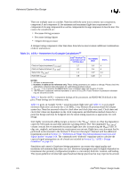
Advanced System Bus Design Term Cross-talk Edge Finger Flight Time GTL+ Definition The reception on a victim network of a signal imposed by aggressor network(s) through inductive and capacitive coupling between the networks. • Backward Cross-talk - coupling which creates a signal in a victim network that travels in the opposite direction as the aggressor's signal. • Forward Cross-talk - coupling which creates a signal in a victim network that travels in the same direction as the aggressor's signal. • Even Mode Cross-talk - coupling from multiple aggressors when all the aggressors switch in the same direction that the victim is switching. • Odd Mode Cross-talk - coupling from multiple aggressors when all the aggressors switch in the opposite direction that the victim is switching. The cartridge electrical contact that interfaces to the SC242 connector. Flight Time is a term in the timing equation that includes the signal propagation delay, any effects the system has on the TCO of the driver, plus any adjustments to the signal at the receiver needed to guarantee the setup time of the receiver. More precisely, flight time is defined to be: • The time difference between a signal at the input pin of a receiving agent crossing VREF (adjusted to meet the receiver manufacturer's conditions required for AC timing specifications; i.e., ringback, etc.), and the output pin of the driving agent crossing VREF if the driver was driving the Test Load used to specify the driver's AC timings. See Section for details regarding flight time simulation and validation. The VREF Guardband takes into account sources of noise that may affect the way an AGTL+ signal becomes valid at the receiver. See the definition of the VREF Guardband. • Maximum and Minimum Flight Time - Flight time variations can be caused by many different parameters. The more obvious causes include variation of the board dielectric constant, changes in load condition, crosstalk, VTT noise, VREF noise, variation in termination resistance and differences in I/O buffer performance as a function of temperature, voltage and manufacturing process. Some less obvious causes include effects of Simultaneous Switching Output (SSO) and packaging effects. • The Maximum Flight Time is the largest flight time a network will experience under all variations of conditions. Maximum flight time is measured at the appropriate VREF Guardband boundary. • The Minimum Flight Time is the smallest flight time a network will experience under all variations of conditions. Minimum flight time is measured at the appropriate VREF Guardband boundary. For more information on flight time and the VREF Guardband, see the Pentium® II Processor Developer's Manual. GTL+ is the bus technology used by the Pentium® Pro processor. This is an incident wave switching, open-drain bus with pull-up resistors that provide both the high logic level and termination. It is an enhancement to the GTL (Gunning Transceiver Logic) technology. See thePentium® II Processor Developer's Manual for more details of GTL+. 3-2 Intel®820 Chipset Design Guide
-
 1
1 -
2
-
3
-
4
-
5
-
6
-
7
-
8
-
9
-
10
-
11
-
12
-
13
-
14
-
15
-
16
-
17
-
18
-
19
-
20
-
21
-
22
-
23
-
24
-
25
-
26
-
27
-
28
-
29
-
30
-
31
-
32
-
33
-
34
-
35
-
36
-
37
-
38
-
39
-
40
-
41
-
42
-
43
-
44
-
45
-
46
-
47
-
48
-
49
-
50
-
51
-
52
-
53
-
54
-
55
-
56
-
57
-
58
-
59
-
60
-
61
-
62
-
63
-
64
-
65
-
66
-
67
-
68
-
69
-
70
-
71
-
72
-
73
-
74
-
75
-
76
-
77
-
78
-
79
-
80
-
81
-
82
-
83
-
84
-
85
-
86
-
87
-
88
-
89
-
90
-
91
-
92
-
93
-
94
-
95
-
96
-
 97
97 -
 98
98 -
 99
99 -
 100
100 -
 101
101 -
 102
102 -
 103
103 -
 104
104 -
 105
105 -
 106
106 -
 107
107 -
108
-
109
-
110
-
111
-
112
-
113
-
114
-
115
-
116
-
117
-
118
-
119
-
120
-
121
-
122
-
123
-
124
-
125
-
126
-
127
-
128
-
129
-
130
-
131
-
132
-
133
-
134
-
135
-
136
-
137
-
138
-
139
-
140
-
141
-
142
-
143
-
144
-
145
-
146
-
147
-
148
-
149
-
150
-
151
-
152
-
153
-
154
-
155
-
156
-
157
-
158
-
159
-
160
-
161
-
162
-
163
-
164
-
165
-
166
-
167
-
168
-
169
-
170
-
171
-
172
-
173
-
174
-
175
-
176
-
177
-
178
-
179
-
180
-
181
-
182
-
183
-
184
-
185
-
186
-
187
-
188
-
189
-
190
-
191
-
192
-
193
-
194
-
195
-
196
-
197
-
198
-
199
-
200
-
201
-
202
-
203
-
204
-
205
-
206
-
207
-
208
-
209
-
210
-
211
-
212
-
213
-
214
-
215
-
216
-
217
-
218
-
219
-
220
-
221
-
222
-
223
-
224
-
225
-
226
-
227
-
228
-
229
-
230
-
231
-
232
-
233
-
234
-
235
-
236
-
237
-
238
-
239
-
240
-
241
-
242
 |
 |
