Intel VC820 Design Guide - Page 48
Equation 2-3. RDRAM Clock Signal Trace Length Calculation
 |
View all Intel VC820 manuals
Add to My Manuals
Save this manual to your list of manuals |
Page 48 highlights
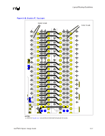
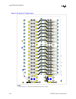
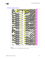
Layout/Routing Guidelines Equation 2-2. RDRAM RSL Signal Trace Length Calculation Package Dimension + Board Trace Length = Nominal RSL Length ± 10mils Figure 2-23. RDRAM Trace Length Matching Example L1, L2 -> Package Dimensions L3, L4 -> Board Trace Length L1 MCH Package MCH Die Ball L3 L2 L4 L1 + L3 = Nominal RSL Length ±10 mils L2 + L4 = Nominal RSL Length ±10 mils R R I I M M M M C C o o n n n n e e c c t t o o V r r t e r m NOTE: Refer to the Intel® 820 Chipset: Intel® 82820 Memory Controller Hub (MCH) Datasheet for component package dimensions. The RDRAM clocks (CTM, CTM#, CFM and CFM#) must be longer than the RDRAM signals due to their increased trace velocity (because they are routed as a differential pair). To calculate the length for each clock, the following formula should be used: Equation 2-3. RDRAM Clock Signal Trace Length Calculation Clock Length = Nominal RSL Signal Length (package + board) * 1.021 Using this formula, the clock signals will be 21 mils/inch longer than the Nominal Length. The lengthening of the clock signals, to compensate for their trace velocity change, ONLY applies to routing between the MCH and the first RIMM. The clock signals should be matched in length to the RSL signals between RIMMs. Refer to Chapter 4, "Clocking" for more detailed clock routing guidelines. The high-speed CMOS signals must be length matched to the RSL signals within 1200 mils (1.2 in) due to a timing requirement between CMOS and RSL signals during NAP Exit and PDN Exit. It is necessary to compensate for the slight difference in electrical characteristics between a dummy via and a real via. Refer to the following section for more information on Via Compensation. 2-22 Intel®820 Chipset Design Guide
-
 1
1 -
2
-
3
-
4
-
5
-
6
-
7
-
8
-
9
-
10
-
11
-
12
-
13
-
14
-
15
-
16
-
17
-
18
-
19
-
20
-
21
-
22
-
23
-
24
-
25
-
26
-
27
-
28
-
29
-
30
-
31
-
32
-
33
-
34
-
35
-
36
-
37
-
38
-
39
-
40
-
41
-
42
-
 43
43 -
 44
44 -
 45
45 -
 46
46 -
 47
47 -
 48
48 -
 49
49 -
 50
50 -
 51
51 -
 52
52 -
 53
53 -
54
-
55
-
56
-
57
-
58
-
59
-
60
-
61
-
62
-
63
-
64
-
65
-
66
-
67
-
68
-
69
-
70
-
71
-
72
-
73
-
74
-
75
-
76
-
77
-
78
-
79
-
80
-
81
-
82
-
83
-
84
-
85
-
86
-
87
-
88
-
89
-
90
-
91
-
92
-
93
-
94
-
95
-
96
-
97
-
98
-
99
-
100
-
101
-
102
-
103
-
104
-
105
-
106
-
107
-
108
-
109
-
110
-
111
-
112
-
113
-
114
-
115
-
116
-
117
-
118
-
119
-
120
-
121
-
122
-
123
-
124
-
125
-
126
-
127
-
128
-
129
-
130
-
131
-
132
-
133
-
134
-
135
-
136
-
137
-
138
-
139
-
140
-
141
-
142
-
143
-
144
-
145
-
146
-
147
-
148
-
149
-
150
-
151
-
152
-
153
-
154
-
155
-
156
-
157
-
158
-
159
-
160
-
161
-
162
-
163
-
164
-
165
-
166
-
167
-
168
-
169
-
170
-
171
-
172
-
173
-
174
-
175
-
176
-
177
-
178
-
179
-
180
-
181
-
182
-
183
-
184
-
185
-
186
-
187
-
188
-
189
-
190
-
191
-
192
-
193
-
194
-
195
-
196
-
197
-
198
-
199
-
200
-
201
-
202
-
203
-
204
-
205
-
206
-
207
-
208
-
209
-
210
-
211
-
212
-
213
-
214
-
215
-
216
-
217
-
218
-
219
-
220
-
221
-
222
-
223
-
224
-
225
-
226
-
227
-
228
-
229
-
230
-
231
-
232
-
233
-
234
-
235
-
236
-
237
-
238
-
239
-
240
-
241
-
242
 |
 |
