Intel VC820 Design Guide - Page 108
Determine General Topology, Layout, and Routing Desired, 3.2.3 Pre-Layout Simulation
 |
View all Intel VC820 manuals
Add to My Manuals
Save this manual to your list of manuals |
Page 108 highlights
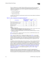
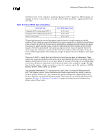
Advanced System Bus Design Table 3-3. Example TFLT_MIN Calculations (Frequency Independent) Driver Processor2 Processor2 82820 MCH Receiver Processor2 82820 MCH Processor2 THOLD 0.8 0.28 0.8 ClkSKEW 0.2 0.2 0.2 TCO_MIN -0.1 -0.1 0.5 Recommended TFLT_MIN 1.2 .58 .5 NOTES: 1. All times in nanoseconds. 2. Processor values specified in this table are examples only. Refer to the appropriate processor datasheet for specification values. 3.2.2 Determine General Topology, Layout, and Routing Desired After calculating the timing budget, determine the approximate location of the processor and the chipset on the base board (see Section 2.9, "System Bus Design" on page 2-46). 3.2.3 Pre-Layout Simulation 3.2.3.1 3.2.3.2 Methodology Analog simulations are recommended for high speed system bus designs. Start simulations prior to layout. Pre-layout simulations provide a detailed picture of the working "solution space" that meets flight time and signal quality requirements. The layout recommendations in the previous sections are based on pre-layout simulations conducted at Intel. By basing board layout guidelines on the solution space, the iterations between layout and post-layout simulation can be reduced. Intel recommends running simulations at the device pads for signal quality and at the device pins for timing analysis. However, simulation results at the device pins may be used later to correlate simulation performance against actual system measurements. Sensitivity Analysis Pre-layout analysis includes a sensitivity analysis using parametric sweeps. Parametric sweep analysis involves varying one or two system parameters while all others such as driver strength, package, Z0, and S0 are held constant. This way, the sensitivity of the proposed bus topology to varying parameters can be analyzed systematically. Sensitivity of the bus to minimum flight time, maximum flight time, and signal quality should be covered. Suggested sweep parameters include trace lengths, termination resistor values, and any other factors that may affect flight time, signal quality, and feasibility of layout. Minimum flight time and worst signal quality are typically analyzed using fast I/O buffers and interconnect. Maximum flight time is typically analyzed using slow I/O buffers and slow interconnects. Outputs from each sweep should be analyzed to determine which regions meet timing and signal quality specifications. To establish the working solution space, find the common space across all the sweeps that result in passing timing and signal quality. The solution space should allow enough design flexibility for a feasible, cost-effective layout. 3-8 Intel®820 Chipset Design Guide
-
 1
1 -
2
-
3
-
4
-
5
-
6
-
7
-
8
-
9
-
10
-
11
-
12
-
13
-
14
-
15
-
16
-
17
-
18
-
19
-
20
-
21
-
22
-
23
-
24
-
25
-
26
-
27
-
28
-
29
-
30
-
31
-
32
-
33
-
34
-
35
-
36
-
37
-
38
-
39
-
40
-
41
-
42
-
43
-
44
-
45
-
46
-
47
-
48
-
49
-
50
-
51
-
52
-
53
-
54
-
55
-
56
-
57
-
58
-
59
-
60
-
61
-
62
-
63
-
64
-
65
-
66
-
67
-
68
-
69
-
70
-
71
-
72
-
73
-
74
-
75
-
76
-
77
-
78
-
79
-
80
-
81
-
82
-
83
-
84
-
85
-
86
-
87
-
88
-
89
-
90
-
91
-
92
-
93
-
94
-
95
-
96
-
97
-
98
-
99
-
100
-
101
-
102
-
 103
103 -
 104
104 -
 105
105 -
 106
106 -
 107
107 -
 108
108 -
 109
109 -
 110
110 -
 111
111 -
 112
112 -
 113
113 -
114
-
115
-
116
-
117
-
118
-
119
-
120
-
121
-
122
-
123
-
124
-
125
-
126
-
127
-
128
-
129
-
130
-
131
-
132
-
133
-
134
-
135
-
136
-
137
-
138
-
139
-
140
-
141
-
142
-
143
-
144
-
145
-
146
-
147
-
148
-
149
-
150
-
151
-
152
-
153
-
154
-
155
-
156
-
157
-
158
-
159
-
160
-
161
-
162
-
163
-
164
-
165
-
166
-
167
-
168
-
169
-
170
-
171
-
172
-
173
-
174
-
175
-
176
-
177
-
178
-
179
-
180
-
181
-
182
-
183
-
184
-
185
-
186
-
187
-
188
-
189
-
190
-
191
-
192
-
193
-
194
-
195
-
196
-
197
-
198
-
199
-
200
-
201
-
202
-
203
-
204
-
205
-
206
-
207
-
208
-
209
-
210
-
211
-
212
-
213
-
214
-
215
-
216
-
217
-
218
-
219
-
220
-
221
-
222
-
223
-
224
-
225
-
226
-
227
-
228
-
229
-
230
-
231
-
232
-
233
-
234
-
235
-
236
-
237
-
238
-
239
-
240
-
241
-
242
 |
 |
