Intel VC820 Design Guide - Page 135
MCH to DRCG, MCH to DRCG Routing Diagram
 |
View all Intel VC820 manuals
Add to My Manuals
Save this manual to your list of manuals |
Page 135 highlights
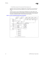
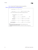
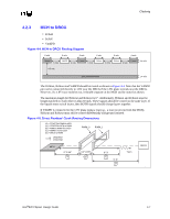
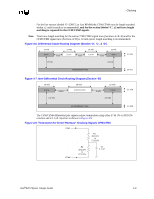
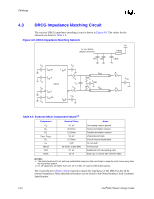
Clocking 4.2.3 MCH to DRCG • PclkM • PclkN • VddIPD Figure 4-4. MCH to DRCG Routing Diagram 6 mils 6 mils 6 mils 6 mils 6 mils 6 mils Ground 6 mils VddiPD 6 mils Ground 6 mils Hclkout 6 mils Rclkout 6 mils Ground 1.4 mils 4.5 mils Ground/Power Plane 1.4 mils The Hclkout, Rclkout and VddiPD should be routed as shown in Figure 4-4. Note that the VddiPD pin can be connected directly to 1.8V near the DRCG if the 1.8V plane extends near the DRCG. However, if a 1.8V trace must be run, it should originate at the MCH and be routed as shown. The maximum length for Hclkout and Rclkout is 6". Additionally, Hclkout and Rclkout must be length matched (to each other) within 50 mils. These signals should be routed on the same layer. If the signals must switch layers, then BOTH signals should change layers together. If VddiPD is connected to the 1.8V plane using a via (e.g., a trace is not run from the MCH), Hclkout and Rclkout must still be routed differentially and ground isolated. Figure 4-5. Direct Rambus* Clock Routing Dimensions (A) = CTM/CTM# RIMM to MCH (A) = CFM/CFM# MCH to RIMM (B) = RIMM to RIMM for Clocks (C) = RIMM to Termination (D) = DRCG to RIMM CFM/CFM# CTM/CTM# RIMM_0 RIMM_1 MCH 0"-3.50" A 0.4"-0.45" B 0"-3" C 0"-6" D Term DRCG b lk t Intel®820 Chipset Design Guide 4-7
-
 1
1 -
2
-
3
-
4
-
5
-
6
-
7
-
8
-
9
-
10
-
11
-
12
-
13
-
14
-
15
-
16
-
17
-
18
-
19
-
20
-
21
-
22
-
23
-
24
-
25
-
26
-
27
-
28
-
29
-
30
-
31
-
32
-
33
-
34
-
35
-
36
-
37
-
38
-
39
-
40
-
41
-
42
-
43
-
44
-
45
-
46
-
47
-
48
-
49
-
50
-
51
-
52
-
53
-
54
-
55
-
56
-
57
-
58
-
59
-
60
-
61
-
62
-
63
-
64
-
65
-
66
-
67
-
68
-
69
-
70
-
71
-
72
-
73
-
74
-
75
-
76
-
77
-
78
-
79
-
80
-
81
-
82
-
83
-
84
-
85
-
86
-
87
-
88
-
89
-
90
-
91
-
92
-
93
-
94
-
95
-
96
-
97
-
98
-
99
-
100
-
101
-
102
-
103
-
104
-
105
-
106
-
107
-
108
-
109
-
110
-
111
-
112
-
113
-
114
-
115
-
116
-
117
-
118
-
119
-
120
-
121
-
122
-
123
-
124
-
125
-
126
-
127
-
128
-
129
-
 130
130 -
 131
131 -
 132
132 -
 133
133 -
 134
134 -
 135
135 -
 136
136 -
 137
137 -
 138
138 -
 139
139 -
 140
140 -
141
-
142
-
143
-
144
-
145
-
146
-
147
-
148
-
149
-
150
-
151
-
152
-
153
-
154
-
155
-
156
-
157
-
158
-
159
-
160
-
161
-
162
-
163
-
164
-
165
-
166
-
167
-
168
-
169
-
170
-
171
-
172
-
173
-
174
-
175
-
176
-
177
-
178
-
179
-
180
-
181
-
182
-
183
-
184
-
185
-
186
-
187
-
188
-
189
-
190
-
191
-
192
-
193
-
194
-
195
-
196
-
197
-
198
-
199
-
200
-
201
-
202
-
203
-
204
-
205
-
206
-
207
-
208
-
209
-
210
-
211
-
212
-
213
-
214
-
215
-
216
-
217
-
218
-
219
-
220
-
221
-
222
-
223
-
224
-
225
-
226
-
227
-
228
-
229
-
230
-
231
-
232
-
233
-
234
-
235
-
236
-
237
-
238
-
239
-
240
-
241
-
242
 |
 |
