Intel VC820 Design Guide - Page 39
Direct Rambus* Ground Plane Reference, Required
 |
View all Intel VC820 manuals
Add to My Manuals
Save this manual to your list of manuals |
Page 39 highlights
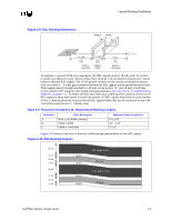
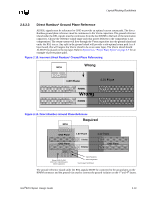
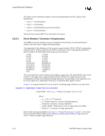
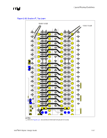
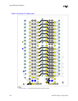
Layout/Routing Guidelines 2.6.2.3 Direct Rambus* Ground Plane Reference All RSL signals must be referenced to GND to provide an optimal current return path. The direct Rambus ground plane reference must be continuous to the Vterm capacitors. The ground reference island under the RSL signals must be continuous from the last RIMM to the back of the termination capacitors. Choose the reference island shape such that power delivery to the components is not compromised. The return current will flow through the Vterm capacitors into the ground island and under the RSL traces. Any split in the ground island will provide a sub-optimal return path. In a 4 layer board, this will require the Vterm island to be on an outer layer. The Vterm island should ALWAYS be placed on the top layer. Refer to Section 6.2, "Power Plane Splits" on page 6-7 for an example of power plane splits. Figure 2-15. Incorrect Direct Rambus* Ground Plane Referencing Wrong MCH 1.8V Plane RIMM1 Wrong RIMM2 3.3V Plane Figure 2-16. Direct Rambus Ground Plane Reference Required MCH GND Plane GND Plane 1.8V Plane RIMM1 RIMM2 3.3V Plane GND Plane Extend GND PLANE Reference Island Beyond Vterm Capacitors Vterm Resistors Vterm Capacitors Vterm Layer Not Shown The ground reference island under the RSL signals MUST be connected to the ground pins on the RIMM connector and the ground vias used to connect the ground isolation on the 1st and 4th layers. Intel®820 Chipset Design Guide 2-13
-
 1
1 -
2
-
3
-
4
-
5
-
6
-
7
-
8
-
9
-
10
-
11
-
12
-
13
-
14
-
15
-
16
-
17
-
18
-
19
-
20
-
21
-
22
-
23
-
24
-
25
-
26
-
27
-
28
-
29
-
30
-
31
-
32
-
33
-
 34
34 -
 35
35 -
 36
36 -
 37
37 -
 38
38 -
 39
39 -
 40
40 -
 41
41 -
 42
42 -
 43
43 -
 44
44 -
45
-
46
-
47
-
48
-
49
-
50
-
51
-
52
-
53
-
54
-
55
-
56
-
57
-
58
-
59
-
60
-
61
-
62
-
63
-
64
-
65
-
66
-
67
-
68
-
69
-
70
-
71
-
72
-
73
-
74
-
75
-
76
-
77
-
78
-
79
-
80
-
81
-
82
-
83
-
84
-
85
-
86
-
87
-
88
-
89
-
90
-
91
-
92
-
93
-
94
-
95
-
96
-
97
-
98
-
99
-
100
-
101
-
102
-
103
-
104
-
105
-
106
-
107
-
108
-
109
-
110
-
111
-
112
-
113
-
114
-
115
-
116
-
117
-
118
-
119
-
120
-
121
-
122
-
123
-
124
-
125
-
126
-
127
-
128
-
129
-
130
-
131
-
132
-
133
-
134
-
135
-
136
-
137
-
138
-
139
-
140
-
141
-
142
-
143
-
144
-
145
-
146
-
147
-
148
-
149
-
150
-
151
-
152
-
153
-
154
-
155
-
156
-
157
-
158
-
159
-
160
-
161
-
162
-
163
-
164
-
165
-
166
-
167
-
168
-
169
-
170
-
171
-
172
-
173
-
174
-
175
-
176
-
177
-
178
-
179
-
180
-
181
-
182
-
183
-
184
-
185
-
186
-
187
-
188
-
189
-
190
-
191
-
192
-
193
-
194
-
195
-
196
-
197
-
198
-
199
-
200
-
201
-
202
-
203
-
204
-
205
-
206
-
207
-
208
-
209
-
210
-
211
-
212
-
213
-
214
-
215
-
216
-
217
-
218
-
219
-
220
-
221
-
222
-
223
-
224
-
225
-
226
-
227
-
228
-
229
-
230
-
231
-
232
-
233
-
234
-
235
-
236
-
237
-
238
-
239
-
240
-
241
-
242
 |
 |
