Intel VC820 Design Guide - Page 110
Place and Route Board, 3.2.4.1 Estimate Component To Component Spacing for AGTL+ Signals
 |
View all Intel VC820 manuals
Add to My Manuals
Save this manual to your list of manuals |
Page 110 highlights
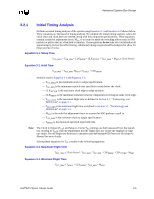
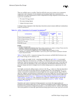
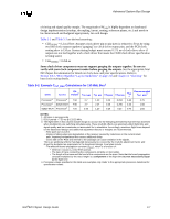
Advanced System Bus Design 3.2.4 3.2.4.1 3.2.4.2 Intel has found wide variation in noise margins when varying the stub impedance and the PCB's Z0 and S0. Intel therefore recommends that PCB parameters are controlled as tightly as possible, with a sampling of the allowable Z0 and S0 simulated. The Intel® Pentium® III processor nominal effective line impedance is 65 Ω ±15%. Future Intel® Pentium® III processor effective line impedance (ZEFF) may be 60 Ω ±15%. Intel recommends the baseboard nominal effective line impedance to be at 60 Ω ±15% for the recommended layout guidelines to be effective. Intel also recommends running uncoupled simulations using the Z0 of the package stubs; and performing fully coupled simulations if increased accuracy is needed or desired. Accounting for cross-talk within the device package by varying the stub impedance was investigated and was not found to be sufficiently accurate. This lead to the development of full package models for the component packages. Place and Route Board Estimate Component To Component Spacing for AGTL+ Signals Estimate the number of layers that will be required. Then determine the expected interconnect distances between each of the components on the AGTL+ bus. Using the estimated interconnect distances, verify that the placement can support the system timing requirements. The required bus frequency and the maximum flight time propagation delay on the PCB determine the maximum network length between the bus agents. The minimum network length is independent of the required bus frequency. Table 3-2 and Table 3-3 assume values for CLKSKEW and CLKJITTER - parameters that are controlled by the system designer. To reduce system clock skew to a minimum, clock buffers that allow their outputs to be tied together are recommended. Intel strongly recommends running analog simulations to ensure that each design has adequate noise and timing margin. Layout and Route Board Route the board satisfying the estimated space and timing requirements. Also stay within the solution space set from the pre-layout sweeps. Estimate the printed circuit board parameters from the placement and other information including the following general guidelines: • Distribute VTT with a power plane or a partial power plane. If this cannot be accomplished, use as wide a trace as possible and route the VTT trace with the same topology as the AGTL+ traces. • Keep the overall length of the bus as short as possible (but do not forget minimum component- to-component distances to meet hold times). • Plan to minimize cross-talk with the following guidelines developed for the example topology given (signal spacing recommendations were based on fully coupled simulations - spacing may be decreased based upon the amount of coupled length): - Use a spacing to line width to dielectric thickness ratio of at least 3:1:2. If εr = 4.5, this should limit coupling to 3.4%. - Minimize the dielectric process variation used in the PCB fabrication. - Eliminate parallel traces between layers not separated by a power or ground plane. Figure 3-3 contains the trace width:space ratios assumed for this topology. The cross-talk cases considered in this guideline involve three types: Intragroup AGTL+, Intergroup AGTL+, and AGTL+ to non-AGTL+. Intra-group AGTL+ cross-talk involves interference between AGTL+ signals within the same group (See Section 3.4, "More Details and Insight" on page 3-19 for a description of the different AGTL+ group types). Intergroup AGTL+ cross-talk involves 3-10 Intel®820 Chipset Design Guide
-
 1
1 -
2
-
3
-
4
-
5
-
6
-
7
-
8
-
9
-
10
-
11
-
12
-
13
-
14
-
15
-
16
-
17
-
18
-
19
-
20
-
21
-
22
-
23
-
24
-
25
-
26
-
27
-
28
-
29
-
30
-
31
-
32
-
33
-
34
-
35
-
36
-
37
-
38
-
39
-
40
-
41
-
42
-
43
-
44
-
45
-
46
-
47
-
48
-
49
-
50
-
51
-
52
-
53
-
54
-
55
-
56
-
57
-
58
-
59
-
60
-
61
-
62
-
63
-
64
-
65
-
66
-
67
-
68
-
69
-
70
-
71
-
72
-
73
-
74
-
75
-
76
-
77
-
78
-
79
-
80
-
81
-
82
-
83
-
84
-
85
-
86
-
87
-
88
-
89
-
90
-
91
-
92
-
93
-
94
-
95
-
96
-
97
-
98
-
99
-
100
-
101
-
102
-
103
-
104
-
 105
105 -
 106
106 -
 107
107 -
 108
108 -
 109
109 -
 110
110 -
 111
111 -
 112
112 -
 113
113 -
 114
114 -
 115
115 -
116
-
117
-
118
-
119
-
120
-
121
-
122
-
123
-
124
-
125
-
126
-
127
-
128
-
129
-
130
-
131
-
132
-
133
-
134
-
135
-
136
-
137
-
138
-
139
-
140
-
141
-
142
-
143
-
144
-
145
-
146
-
147
-
148
-
149
-
150
-
151
-
152
-
153
-
154
-
155
-
156
-
157
-
158
-
159
-
160
-
161
-
162
-
163
-
164
-
165
-
166
-
167
-
168
-
169
-
170
-
171
-
172
-
173
-
174
-
175
-
176
-
177
-
178
-
179
-
180
-
181
-
182
-
183
-
184
-
185
-
186
-
187
-
188
-
189
-
190
-
191
-
192
-
193
-
194
-
195
-
196
-
197
-
198
-
199
-
200
-
201
-
202
-
203
-
204
-
205
-
206
-
207
-
208
-
209
-
210
-
211
-
212
-
213
-
214
-
215
-
216
-
217
-
218
-
219
-
220
-
221
-
222
-
223
-
224
-
225
-
226
-
227
-
228
-
229
-
230
-
231
-
232
-
233
-
234
-
235
-
236
-
237
-
238
-
239
-
240
-
241
-
242
 |
 |
