Intel VC820 Design Guide - Page 138
DRCG Impedance Matching Circuit, DRCG Impedance Matching Network
 |
View all Intel VC820 manuals
Add to My Manuals
Save this manual to your list of manuals |
Page 138 highlights
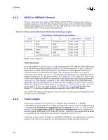
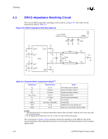
Clocking 4.3 DRCG Impedance Matching Circuit The external DRCG impedance matching circuit is shown in Figure 4-9. The values for the elements are listed in Table 4-5. Figure 4-9. DRCG Impedance Matching Network To 3.3V DRCG Supply Connection 3.3v FBead CD V DD IR CD V DDO V DD P CD DRCG CD V DD C V DD IPD CD VDDO R S CF R S CD CD2 CD2 ZCH R P C MID R P ZCH CBulk RT CMID2 RT Table 4-5. External DRCG Component Values1,2 Component CD RS RP CMID, CMID2 RT CF FBead CD2 CBulk Nominal Value 0.1 uF 39 Ohms 51 Ohms 0.1 uF 27 Ohms 4 pF 50 Ohms at 100 MHz 0.1 uF 10 uF Notes Decoupling caps to ground Series termination resistor Parallel termination resistor Virtual ground caps End of channel termination Do not stuff Ferrite bead Additional 3.3V decoupling caps Bulk cap on device side of ferrite bead NOTES: 1. The ferrite bead and 10 uF bulk cap combination improves jitter and helps to keep the clock noise away from the rest of the system. 2. 0.1 uF capacitors are better than 0.01 uF or 0.001 uF caps for DRCG decoupling. The circuit shown in Figure 4-9 is required to match the impedance of the DRCG to the 28 Ω channel impedance. More detailed information can be found in the Direct Rambus Clock Generator Specification. 4-10 Intel®820 Chipset Design Guide
-
 1
1 -
2
-
3
-
4
-
5
-
6
-
7
-
8
-
9
-
10
-
11
-
12
-
13
-
14
-
15
-
16
-
17
-
18
-
19
-
20
-
21
-
22
-
23
-
24
-
25
-
26
-
27
-
28
-
29
-
30
-
31
-
32
-
33
-
34
-
35
-
36
-
37
-
38
-
39
-
40
-
41
-
42
-
43
-
44
-
45
-
46
-
47
-
48
-
49
-
50
-
51
-
52
-
53
-
54
-
55
-
56
-
57
-
58
-
59
-
60
-
61
-
62
-
63
-
64
-
65
-
66
-
67
-
68
-
69
-
70
-
71
-
72
-
73
-
74
-
75
-
76
-
77
-
78
-
79
-
80
-
81
-
82
-
83
-
84
-
85
-
86
-
87
-
88
-
89
-
90
-
91
-
92
-
93
-
94
-
95
-
96
-
97
-
98
-
99
-
100
-
101
-
102
-
103
-
104
-
105
-
106
-
107
-
108
-
109
-
110
-
111
-
112
-
113
-
114
-
115
-
116
-
117
-
118
-
119
-
120
-
121
-
122
-
123
-
124
-
125
-
126
-
127
-
128
-
129
-
130
-
131
-
132
-
 133
133 -
 134
134 -
 135
135 -
 136
136 -
 137
137 -
 138
138 -
 139
139 -
 140
140 -
 141
141 -
 142
142 -
 143
143 -
144
-
145
-
146
-
147
-
148
-
149
-
150
-
151
-
152
-
153
-
154
-
155
-
156
-
157
-
158
-
159
-
160
-
161
-
162
-
163
-
164
-
165
-
166
-
167
-
168
-
169
-
170
-
171
-
172
-
173
-
174
-
175
-
176
-
177
-
178
-
179
-
180
-
181
-
182
-
183
-
184
-
185
-
186
-
187
-
188
-
189
-
190
-
191
-
192
-
193
-
194
-
195
-
196
-
197
-
198
-
199
-
200
-
201
-
202
-
203
-
204
-
205
-
206
-
207
-
208
-
209
-
210
-
211
-
212
-
213
-
214
-
215
-
216
-
217
-
218
-
219
-
220
-
221
-
222
-
223
-
224
-
225
-
226
-
227
-
228
-
229
-
230
-
231
-
232
-
233
-
234
-
235
-
236
-
237
-
238
-
239
-
240
-
241
-
242
 |
 |
