Intel VC820 Design Guide - Page 32
Data Strobing Example, Effect of Crosstalk on Strobe Signal
 |
View all Intel VC820 manuals
Add to My Manuals
Save this manual to your list of manuals |
Page 32 highlights
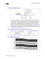
Layout/Routing Guidelines Figure 2-6. Data Strobing Example Data Sample Clock Strobe Data data_str.vsd For a source synchronous strobed interface, it is very important that the strobe signals are routed carefully. These signals must be very clean (free of noise). Data signals are typically latched on the rising or falling edge of the strobe signal (or both). If there is noise on these signals, it could cause an extra "edge" to be detected, thus latching incorrect data. Refer to Figure 2-7 for examples. Figure 2-7. Effect of Crosstalk on Strobe Signal a) Correct Strobing Example (no noise) b) Effect of Crosstalk on Strobe Signal clock Data Data is correctly latchecd as a "0" clock Data Data is incorrectly latchecd as a "1" Noise (i.e., crosstalk) Threshold Threshold Strobe Strobe Some buses have more than one strobe (i.e., AGP). The AGP 1.0 specification (1X and 2X mode) employs 3 strobe signals. These three strobe signals are each used to strobe different data signals. That is, each strobe has an associated set of data signals. The associations for AGP 1.0 (AGP 2X) are documented in Table 2-1. Refer to Section 2.7, "AGP 2.0" on page 2-31 for more information on AGP 2.0 (AGP 4X, 1.5v). Table 2-1. AGP 2X Data/Strobe Association Data Associated Strobe AD[15:0] and C/BE[1:0]# AD[31:16] and C/BE[3:2]# SBA[7:0] AD_STB0 AD_STB1 SB_STB In this example, the lower address signals (AD[15:0]) are sampled on the rising and falling edges of AD_STB0, while the upper address signals (AD[31:16]) are sampled on the rising and falling edges of AD_STB1. 2-6 Intel®820 Chipset Design Guide
-
 1
1 -
2
-
3
-
4
-
5
-
6
-
7
-
8
-
9
-
10
-
11
-
12
-
13
-
14
-
15
-
16
-
17
-
18
-
19
-
20
-
21
-
22
-
23
-
24
-
25
-
26
-
 27
27 -
 28
28 -
 29
29 -
 30
30 -
 31
31 -
 32
32 -
 33
33 -
 34
34 -
 35
35 -
 36
36 -
 37
37 -
38
-
39
-
40
-
41
-
42
-
43
-
44
-
45
-
46
-
47
-
48
-
49
-
50
-
51
-
52
-
53
-
54
-
55
-
56
-
57
-
58
-
59
-
60
-
61
-
62
-
63
-
64
-
65
-
66
-
67
-
68
-
69
-
70
-
71
-
72
-
73
-
74
-
75
-
76
-
77
-
78
-
79
-
80
-
81
-
82
-
83
-
84
-
85
-
86
-
87
-
88
-
89
-
90
-
91
-
92
-
93
-
94
-
95
-
96
-
97
-
98
-
99
-
100
-
101
-
102
-
103
-
104
-
105
-
106
-
107
-
108
-
109
-
110
-
111
-
112
-
113
-
114
-
115
-
116
-
117
-
118
-
119
-
120
-
121
-
122
-
123
-
124
-
125
-
126
-
127
-
128
-
129
-
130
-
131
-
132
-
133
-
134
-
135
-
136
-
137
-
138
-
139
-
140
-
141
-
142
-
143
-
144
-
145
-
146
-
147
-
148
-
149
-
150
-
151
-
152
-
153
-
154
-
155
-
156
-
157
-
158
-
159
-
160
-
161
-
162
-
163
-
164
-
165
-
166
-
167
-
168
-
169
-
170
-
171
-
172
-
173
-
174
-
175
-
176
-
177
-
178
-
179
-
180
-
181
-
182
-
183
-
184
-
185
-
186
-
187
-
188
-
189
-
190
-
191
-
192
-
193
-
194
-
195
-
196
-
197
-
198
-
199
-
200
-
201
-
202
-
203
-
204
-
205
-
206
-
207
-
208
-
209
-
210
-
211
-
212
-
213
-
214
-
215
-
216
-
217
-
218
-
219
-
220
-
221
-
222
-
223
-
224
-
225
-
226
-
227
-
228
-
229
-
230
-
231
-
232
-
233
-
234
-
235
-
236
-
237
-
238
-
239
-
240
-
241
-
242
 |
 |
