Intel VC820 Design Guide - Page 27
Layout/Routing Guidelines 2, 2.1 General Recommendations, 2.2 Component Quadrant Layout
 |
View all Intel VC820 manuals
Add to My Manuals
Save this manual to your list of manuals |
Page 27 highlights
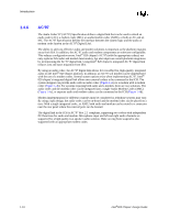
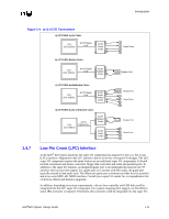
Layout/Routing Guidelines Layout/Routing Guidelines 2 This chapter documents motherboard layout and routing guidelines for Intel® 820 chipset based systems. This section does not discuss the functional aspects of any bus, or the layout guidelines for an add-in device. Caution: If the guidelines listed in this document are not followed, it is very important that thorough signal integrity and timing simulations are completed for each design. Even when the guidelines are followed, critical signals should still be simulated to ensure proper signal integrity and flight time. As bus speeds increase, it is imperative that the guidelines documented are followed precisely. Any deviation from these guidelines must be simulated! 2.1 General Recommendations The trace impedance typically noted (i.e., 60 Ω ±10%) is the "nominal" trace impedance. That is, the impedance of the trace when not subjected to the fields created by changing current in neighboring traces. When calculating flight times, it is important to consider the minimum and maximum impedance of a trace based on the switching of neighboring traces. Using wider spaces between the traces can minimize this trace-to-trace coupling. In addition, these wider spaces reduce crosstalk and settling time. Coupling between two traces is a function of the coupled length, the distance separating the traces, the signal edge rate, and the degree of mutual capacitance and inductance. In order to minimize the effects of trace-to-trace coupling, the routing guidelines documented in this section should be followed. In addition, the PCB should be fabricated as documented in Section 5.3, "Stackup Requirement" on page 5-1 of this document. All recommendations in this section (except where noted) assume 5 mil wide traces. If trace width is greater than 5 mils then the trace spacing requirements must be adjusted accordingly (linearly). For example, this section recommends routing most AGP signals with 5 mil traces on 20 mil spaces (1:4). If 6 mil traces are used, then 24 mil spaces must be used (also 1:4). Using a wider trace (and therefore wider spaces) will make routing more difficult. Additionally, these routing guidelines are created using the stack-up described in section Section 5.3, "Stackup Requirement" on page 5-1. If this stack-up is not used, extremely thorough simulations of every interface must be completed. Using a thicker dielectric (prepreg) will make routing very difficult or impossible. 2.2 Component Quadrant Layout The quadrant layouts shown are approximate and the exact ball assignments should be used to conduct routing analysis. These quadrant layouts are designed for use during component placement. Intel®820 Chipset Design Guide 2-1
-
 1
1 -
2
-
3
-
4
-
5
-
6
-
7
-
8
-
9
-
10
-
11
-
12
-
13
-
14
-
15
-
16
-
17
-
18
-
19
-
20
-
21
-
 22
22 -
 23
23 -
 24
24 -
 25
25 -
 26
26 -
 27
27 -
 28
28 -
 29
29 -
 30
30 -
 31
31 -
 32
32 -
33
-
34
-
35
-
36
-
37
-
38
-
39
-
40
-
41
-
42
-
43
-
44
-
45
-
46
-
47
-
48
-
49
-
50
-
51
-
52
-
53
-
54
-
55
-
56
-
57
-
58
-
59
-
60
-
61
-
62
-
63
-
64
-
65
-
66
-
67
-
68
-
69
-
70
-
71
-
72
-
73
-
74
-
75
-
76
-
77
-
78
-
79
-
80
-
81
-
82
-
83
-
84
-
85
-
86
-
87
-
88
-
89
-
90
-
91
-
92
-
93
-
94
-
95
-
96
-
97
-
98
-
99
-
100
-
101
-
102
-
103
-
104
-
105
-
106
-
107
-
108
-
109
-
110
-
111
-
112
-
113
-
114
-
115
-
116
-
117
-
118
-
119
-
120
-
121
-
122
-
123
-
124
-
125
-
126
-
127
-
128
-
129
-
130
-
131
-
132
-
133
-
134
-
135
-
136
-
137
-
138
-
139
-
140
-
141
-
142
-
143
-
144
-
145
-
146
-
147
-
148
-
149
-
150
-
151
-
152
-
153
-
154
-
155
-
156
-
157
-
158
-
159
-
160
-
161
-
162
-
163
-
164
-
165
-
166
-
167
-
168
-
169
-
170
-
171
-
172
-
173
-
174
-
175
-
176
-
177
-
178
-
179
-
180
-
181
-
182
-
183
-
184
-
185
-
186
-
187
-
188
-
189
-
190
-
191
-
192
-
193
-
194
-
195
-
196
-
197
-
198
-
199
-
200
-
201
-
202
-
203
-
204
-
205
-
206
-
207
-
208
-
209
-
210
-
211
-
212
-
213
-
214
-
215
-
216
-
217
-
218
-
219
-
220
-
221
-
222
-
223
-
224
-
225
-
226
-
227
-
228
-
229
-
230
-
231
-
232
-
233
-
234
-
235
-
236
-
237
-
238
-
239
-
240
-
241
-
242
 |
 |
