Intel VC820 Design Guide - Page 104
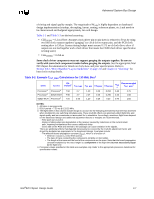
AGTL+ Design Guidelines, Inter-Symbol Interference ISI, Cross-talk, and Monte Carlo Analysis
 |
View all Intel VC820 manuals
Add to My Manuals
Save this manual to your list of manuals |
Page 104 highlights
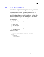
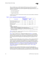
Advanced System Bus Design 3.2 AGTL+ Design Guidelines The following step-by-step guideline was developed for systems based on two processor loads and one Intel 82820 MCH load. Systems using custom chipsets will require timing analysis and analog simulations specific to those components. The guideline recommended in this section is based on experience developed at Intel while developing many different Intel Pentium® Pro processor family and Intel Pentium III processorbased systems. Begin with an initial timing analysis and topology definition. Perform pre-layout analog simulations for a detailed picture of a working "solution space" for the design. These prelayout simulations help define routing rules prior to placement and routing. After routing, extract the interconnect database and perform post-layout simulations to refine the timing and signal integrity analysis. Validate the analog simulations when actual systems become available. The validation section describes a method for determining the flight time in the actual system. Guideline Methodology: • Initial Timing Analysis • Determine General Topology, Layout, and Routing • Pre-Layout Simulation - Sensitivity sweep - Monte Carlo Analysis • Place and Route Board - Estimate Component to Component Spacing for AGTL+ Signals - Layout and Route Board • Post-Layout Simulation - Interconnect Extraction - Inter-Symbol Interference (ISI), Cross-talk, and Monte Carlo Analysis • Validation - Measurements - Determining Flight Time 3-4 Intel®820 Chipset Design Guide
-
 1
1 -
2
-
3
-
4
-
5
-
6
-
7
-
8
-
9
-
10
-
11
-
12
-
13
-
14
-
15
-
16
-
17
-
18
-
19
-
20
-
21
-
22
-
23
-
24
-
25
-
26
-
27
-
28
-
29
-
30
-
31
-
32
-
33
-
34
-
35
-
36
-
37
-
38
-
39
-
40
-
41
-
42
-
43
-
44
-
45
-
46
-
47
-
48
-
49
-
50
-
51
-
52
-
53
-
54
-
55
-
56
-
57
-
58
-
59
-
60
-
61
-
62
-
63
-
64
-
65
-
66
-
67
-
68
-
69
-
70
-
71
-
72
-
73
-
74
-
75
-
76
-
77
-
78
-
79
-
80
-
81
-
82
-
83
-
84
-
85
-
86
-
87
-
88
-
89
-
90
-
91
-
92
-
93
-
94
-
95
-
96
-
97
-
98
-
 99
99 -
 100
100 -
 101
101 -
 102
102 -
 103
103 -
 104
104 -
 105
105 -
 106
106 -
 107
107 -
 108
108 -
 109
109 -
110
-
111
-
112
-
113
-
114
-
115
-
116
-
117
-
118
-
119
-
120
-
121
-
122
-
123
-
124
-
125
-
126
-
127
-
128
-
129
-
130
-
131
-
132
-
133
-
134
-
135
-
136
-
137
-
138
-
139
-
140
-
141
-
142
-
143
-
144
-
145
-
146
-
147
-
148
-
149
-
150
-
151
-
152
-
153
-
154
-
155
-
156
-
157
-
158
-
159
-
160
-
161
-
162
-
163
-
164
-
165
-
166
-
167
-
168
-
169
-
170
-
171
-
172
-
173
-
174
-
175
-
176
-
177
-
178
-
179
-
180
-
181
-
182
-
183
-
184
-
185
-
186
-
187
-
188
-
189
-
190
-
191
-
192
-
193
-
194
-
195
-
196
-
197
-
198
-
199
-
200
-
201
-
202
-
203
-
204
-
205
-
206
-
207
-
208
-
209
-
210
-
211
-
212
-
213
-
214
-
215
-
216
-
217
-
218
-
219
-
220
-
221
-
222
-
223
-
224
-
225
-
226
-
227
-
228
-
229
-
230
-
231
-
232
-
233
-
234
-
235
-
236
-
237
-
238
-
239
-
240
-
241
-
242
 |
 |
