Intel VC820 Design Guide - Page 49
VIA Compensation, 2.6.2.8 Length Matching & Via Compensation Example
 |
View all Intel VC820 manuals
Add to My Manuals
Save this manual to your list of manuals |
Page 49 highlights
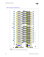
Layout/Routing Guidelines 2.6.2.7 VIA Compensation As described in Section 2.8.2, "Strobe Signals" on page 2-44, all signals must have the same number of vias. As a result, each trace will have 1 via (near the BGA pad) because some of the RSL signals must be routed on the bottom of the motherboard. Therefore, it is necessary to place a dummy via on all signals that are routed on the top layer. Because the electrical characteristics of a dummy via do not match the electrical characteristics of a real via exactly, additional compensation must be performed on each signal that has a dummy via. Each signal with a dummy via must have 25 mils of additional trace length. That is: a real via = a dummy via + 25 mils of trace length. This 25 mils of additional trace length must be added to each signal routed on the top layer after length matching, as documented in Section 2.6.2.6, "Length Matching Methods" on page 2-21. Figure 2-24. "Dummy" Via vs. Real "Via" "DUMMY Via" Trace "REAL Via" Trace PCB PCB PCB PCB Via Via Trace 2.6.2.8 Length Matching & Via Compensation Example Table 2-5 can be used to ensure that the RSL signals are the correct length. Note: 2000 mils was chosen as an EXAMPLE Nominal RSL Length. Intel®820 Chipset Design Guide 2-23
-
 1
1 -
2
-
3
-
4
-
5
-
6
-
7
-
8
-
9
-
10
-
11
-
12
-
13
-
14
-
15
-
16
-
17
-
18
-
19
-
20
-
21
-
22
-
23
-
24
-
25
-
26
-
27
-
28
-
29
-
30
-
31
-
32
-
33
-
34
-
35
-
36
-
37
-
38
-
39
-
40
-
41
-
42
-
43
-
 44
44 -
 45
45 -
 46
46 -
 47
47 -
 48
48 -
 49
49 -
 50
50 -
 51
51 -
 52
52 -
 53
53 -
 54
54 -
55
-
56
-
57
-
58
-
59
-
60
-
61
-
62
-
63
-
64
-
65
-
66
-
67
-
68
-
69
-
70
-
71
-
72
-
73
-
74
-
75
-
76
-
77
-
78
-
79
-
80
-
81
-
82
-
83
-
84
-
85
-
86
-
87
-
88
-
89
-
90
-
91
-
92
-
93
-
94
-
95
-
96
-
97
-
98
-
99
-
100
-
101
-
102
-
103
-
104
-
105
-
106
-
107
-
108
-
109
-
110
-
111
-
112
-
113
-
114
-
115
-
116
-
117
-
118
-
119
-
120
-
121
-
122
-
123
-
124
-
125
-
126
-
127
-
128
-
129
-
130
-
131
-
132
-
133
-
134
-
135
-
136
-
137
-
138
-
139
-
140
-
141
-
142
-
143
-
144
-
145
-
146
-
147
-
148
-
149
-
150
-
151
-
152
-
153
-
154
-
155
-
156
-
157
-
158
-
159
-
160
-
161
-
162
-
163
-
164
-
165
-
166
-
167
-
168
-
169
-
170
-
171
-
172
-
173
-
174
-
175
-
176
-
177
-
178
-
179
-
180
-
181
-
182
-
183
-
184
-
185
-
186
-
187
-
188
-
189
-
190
-
191
-
192
-
193
-
194
-
195
-
196
-
197
-
198
-
199
-
200
-
201
-
202
-
203
-
204
-
205
-
206
-
207
-
208
-
209
-
210
-
211
-
212
-
213
-
214
-
215
-
216
-
217
-
218
-
219
-
220
-
221
-
222
-
223
-
224
-
225
-
226
-
227
-
228
-
229
-
230
-
231
-
232
-
233
-
234
-
235
-
236
-
237
-
238
-
239
-
240
-
241
-
242
 |
 |
