Intel VC820 Design Guide - Page 130
Intel, Chipset Platform Clock Distribution
 |
View all Intel VC820 manuals
Add to My Manuals
Save this manual to your list of manuals |
Page 130 highlights
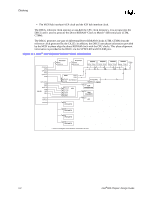
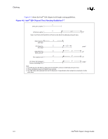
Clocking • The MCH hub interface/AGP clock and the ICH hub interface clock. The DRCG reference clock operates at one-half the CPU clock frequency. It is an input into the DRCG and is used to generate the Direct RDRAM "Clock to Master" differential pair (CTM, CTM#). The DRCG generates one pair of differential Direct RDRAM Clocks (CTM, CTM#) from the reference clock generated by the CK133. In addition, the DRCG uses phase information provided by the MCH to phase align the direct RDRAM clock with the CPU clocks. This phase alignment information is provided to the DRCG via the SYNCLKN and PCLKM pins. Figure 4-1. Intel® 820 Chipset Platform Clock Distribution CPUCLK APIC CPUCLK APIC CPUCLK 3V66 CPU_DIV2 3V66 APIC PCICLK* 3V66 CK133 REF 48Hz PCICLK PCICLK PCICLK Processor A CLK B PICCLK Processor C CLK D PICCLK RDRAM RCLK TCLK RDRAM RCLK TCLK RDRAM RCLK TCLK RDRAM TERM RCLK TCLK MCH CTM CFM E F HCLKIN CLK66 PHASEINFO G APICCLK ICH H PCICLK I CLK66 J CLK14 K CLK48 L CLK PCI SLOTS L CLK PCI SLOTS L CLK PCI SLOTS L CLK PCI SLOTS PHASEINFO Q REFCLK DRCG P CLK AGP CONNECTOR N CLK FWH Flash BIOS M CLK LPC * The free-running PCI clock should be connected to the ICH. 4-2 Intel®820 Chipset Design Guide
-
 1
1 -
2
-
3
-
4
-
5
-
6
-
7
-
8
-
9
-
10
-
11
-
12
-
13
-
14
-
15
-
16
-
17
-
18
-
19
-
20
-
21
-
22
-
23
-
24
-
25
-
26
-
27
-
28
-
29
-
30
-
31
-
32
-
33
-
34
-
35
-
36
-
37
-
38
-
39
-
40
-
41
-
42
-
43
-
44
-
45
-
46
-
47
-
48
-
49
-
50
-
51
-
52
-
53
-
54
-
55
-
56
-
57
-
58
-
59
-
60
-
61
-
62
-
63
-
64
-
65
-
66
-
67
-
68
-
69
-
70
-
71
-
72
-
73
-
74
-
75
-
76
-
77
-
78
-
79
-
80
-
81
-
82
-
83
-
84
-
85
-
86
-
87
-
88
-
89
-
90
-
91
-
92
-
93
-
94
-
95
-
96
-
97
-
98
-
99
-
100
-
101
-
102
-
103
-
104
-
105
-
106
-
107
-
108
-
109
-
110
-
111
-
112
-
113
-
114
-
115
-
116
-
117
-
118
-
119
-
120
-
121
-
122
-
123
-
124
-
 125
125 -
 126
126 -
 127
127 -
 128
128 -
 129
129 -
 130
130 -
 131
131 -
 132
132 -
 133
133 -
 134
134 -
 135
135 -
136
-
137
-
138
-
139
-
140
-
141
-
142
-
143
-
144
-
145
-
146
-
147
-
148
-
149
-
150
-
151
-
152
-
153
-
154
-
155
-
156
-
157
-
158
-
159
-
160
-
161
-
162
-
163
-
164
-
165
-
166
-
167
-
168
-
169
-
170
-
171
-
172
-
173
-
174
-
175
-
176
-
177
-
178
-
179
-
180
-
181
-
182
-
183
-
184
-
185
-
186
-
187
-
188
-
189
-
190
-
191
-
192
-
193
-
194
-
195
-
196
-
197
-
198
-
199
-
200
-
201
-
202
-
203
-
204
-
205
-
206
-
207
-
208
-
209
-
210
-
211
-
212
-
213
-
214
-
215
-
216
-
217
-
218
-
219
-
220
-
221
-
222
-
223
-
224
-
225
-
226
-
227
-
228
-
229
-
230
-
231
-
232
-
233
-
234
-
235
-
236
-
237
-
238
-
239
-
240
-
241
-
242
 |
 |
