Intel VC820 Design Guide - Page 136
DRCG to RDRAM Channel, 4.2.5 Trace Length, Trace Geometry
 |
View all Intel VC820 manuals
Add to My Manuals
Save this manual to your list of manuals |
Page 136 highlights
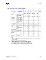
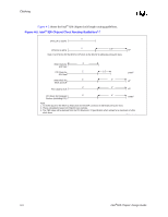
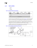
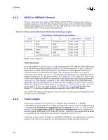
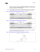
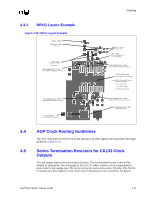
Clocking 4.2.4 DRCG to RDRAM Channel The Direct Rambus* clock signals (CTM/CTM# and CFM/CFM#) are high-speed, impedance matched transmission lines. The Direct Rambus* clocks begin at the end of the Direct Rambus* channel and propagate to the controller as CTM/CTM# (see Figure 4-5), where it loops back as CFM/CFM#. Table 4-4 lists the placement guidelines. Table 4-4. Placement Guidelines for Motherboard Routing Lengths Direct Rambus* Clock Routing Length Guidelines Clock CTM/CTM# CFM/CFM# From DRCG RIMM 1st RIMM Connector Chipset RIMM Last RIMM Connector To Last RIMM Connector RIMM Chipset 1st RIMM Connector RIMM Termination Length (inches) 0.000 - 6.000 0.400 - 0.450 0.000 - 3.500 0.000 - 3.500 0.400 - 0.450 0.000 - 3.000 Section* D B A A B C NOTE: * Refer to Figure 4-5 Trace Geometry In Sections labeled 'A' and 'D' (Figure 4-5) the clock signals (CTM/CTM# and CFM/CFM#) must be 14 mils wide and routed as shown in Figure 4-6. For all other sections ('B' and 'C') the clock signals must be routed with 18 mil wide traces. There must be a 22 mil ground isolation trace routed around the clock differential pair signals. The 22 mil ground isolation traces must be connected to ground with a via every 1". A 6 mil gap is required between the clock signals and the ground isolation traces. For the section labeled "A" in Figure 4-5, 0.021 inches of CLK per 1 inch of RSL trace length must be added to compensate for the clocks faster trace velocity as described in Section 2.6.2.1, "RSL Routing" on page 2-8. The CTM/CTM# and the CFM/CFM# differential signal pairs must be length matched to ±2 mils in line section labeled 'A' and for the line sections labeled 'B' using the trace length methods in Section 2.6.2.1, "RSL Routing" on page 2-8. For the section labeled 'D' the trace length matching for CTM/CTM# is ±2 mils, and for the section labeled 'C', ±2 mil trace length matching is required for the CFM/CFM# signals. The CTM/CTM# signals must be ground referenced (with a continuous ground island/plane) from the DRCG to the Last RIMM. 4.2.5 Trace Length For the section labeled "A" in Figure 4-5 (1st RIMM to MCH and MCH to 1st RIMM), CTM/CTM# and CFM/CFM# must be length matched within ±2 mils (exact trace length matching is recommended). Package trace compensation (as described in Section 2.6.2.1, "RSL Routing" on page 2-8), via compensation, and RSL signal layer alternation must also be completed on the clock signals. Additionally, 0.021 inches of CLK per 1 inch of RSL trace length must be added to compensate for the clocks faster trace velocity as described in Section 2.6.2.1. For the line sections labeled 'B' (Figure 4-5) (RIMM to RIMM) the clock signals must be matched within ±2 mils to the trace length of every RSL signal. Exact length matching is preferred. 4-8 Intel®820 Chipset Design Guide
-
 1
1 -
2
-
3
-
4
-
5
-
6
-
7
-
8
-
9
-
10
-
11
-
12
-
13
-
14
-
15
-
16
-
17
-
18
-
19
-
20
-
21
-
22
-
23
-
24
-
25
-
26
-
27
-
28
-
29
-
30
-
31
-
32
-
33
-
34
-
35
-
36
-
37
-
38
-
39
-
40
-
41
-
42
-
43
-
44
-
45
-
46
-
47
-
48
-
49
-
50
-
51
-
52
-
53
-
54
-
55
-
56
-
57
-
58
-
59
-
60
-
61
-
62
-
63
-
64
-
65
-
66
-
67
-
68
-
69
-
70
-
71
-
72
-
73
-
74
-
75
-
76
-
77
-
78
-
79
-
80
-
81
-
82
-
83
-
84
-
85
-
86
-
87
-
88
-
89
-
90
-
91
-
92
-
93
-
94
-
95
-
96
-
97
-
98
-
99
-
100
-
101
-
102
-
103
-
104
-
105
-
106
-
107
-
108
-
109
-
110
-
111
-
112
-
113
-
114
-
115
-
116
-
117
-
118
-
119
-
120
-
121
-
122
-
123
-
124
-
125
-
126
-
127
-
128
-
129
-
130
-
 131
131 -
 132
132 -
 133
133 -
 134
134 -
 135
135 -
 136
136 -
 137
137 -
 138
138 -
 139
139 -
 140
140 -
 141
141 -
142
-
143
-
144
-
145
-
146
-
147
-
148
-
149
-
150
-
151
-
152
-
153
-
154
-
155
-
156
-
157
-
158
-
159
-
160
-
161
-
162
-
163
-
164
-
165
-
166
-
167
-
168
-
169
-
170
-
171
-
172
-
173
-
174
-
175
-
176
-
177
-
178
-
179
-
180
-
181
-
182
-
183
-
184
-
185
-
186
-
187
-
188
-
189
-
190
-
191
-
192
-
193
-
194
-
195
-
196
-
197
-
198
-
199
-
200
-
201
-
202
-
203
-
204
-
205
-
206
-
207
-
208
-
209
-
210
-
211
-
212
-
213
-
214
-
215
-
216
-
217
-
218
-
219
-
220
-
221
-
222
-
223
-
224
-
225
-
226
-
227
-
228
-
229
-
230
-
231
-
232
-
233
-
234
-
235
-
236
-
237
-
238
-
239
-
240
-
241
-
242
 |
 |
