Intel VC820 Design Guide - Page 106
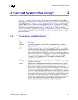
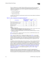
Table 3-1. AGTL+ Parameters for Example Calculations,
 |
View all Intel VC820 manuals
Add to My Manuals
Save this manual to your list of manuals |
Page 106 highlights
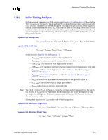
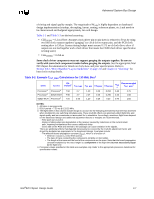
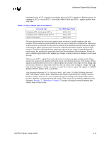
Advanced System Bus Design There are multiple cases to consider. Note that while the same trace connects two components, component A and component B, the minimum and maximum flight time requirements for component A driving component B as well as component B driving component A must be met. The cases to be considered are: • Processor driving processor • Processor driving chipset • Chipset driving processor A designer using components other than those listed above must evaluate additional combinations of driver and receiver. Table 3-1. AGTL+ Parameters for Example Calculations1,2 IC Parameters Intel® Pentium® III processor core at 133 MHz Bus Clock to Output maximum (TCO_MAX) 2.7 Clock to Output minimum (TCO_MIN) -0.1 Setup time (TSU_MIN) 1.2 Hold time (THOLD) 0.8 Intel 82820 MCH 3.6 0.5 2.27 0.28 Notes 4 4 3,4 4 NOTES: 1. All times in nanoseconds. 2. Numbers in table are for reference only. These timing parameters are subject to change. Please check the appropriate component documentation for valid timing parameter values. 3. TSU_MIN = 1.9 ns assumes the 82820 MCH sees a minimum edge rate equal to 0.3 V/ns. 4. The Pentium III substrate nominal impedance is set to 65 Ω ±15%. Future Pentium III processor substrate may be set at 60 Ω ±15% Table 3-1 lists the AGTL+ component timings of the processors and 82820 MCH defined at the pins. These timings are for reference only. Table 3-2 gives an example AGTL+ initial maximum flight time and Table 3-3 is an example minimum flight time calculation for a 133 MHz, 2-way Pentium III processor/Intel 820 chipset system bus. Note that assumed values for clock skew and clock jitter were used. Clock skew and clock jitter values are dependent on the clock components and distribution method chosen for a particular design and must be budgeted into the initial timing equations as appropriate for each design. Intel highly recommends adding margin as shown in the "MADJ" column to offset the degradation caused by SSO push-out and other multi-bit switching effects. The "Recommended TFLT_MAX" column contains the recommended maximum flight time after incorporating the MADJ value. If edge rate, ringback, and monotonicity requirements are not met, flight time correction must first be performed as documented in the Pentium® II Processor Developer's Manual with the additional requirements noted in Section 3.5, "Definitions of Flight Time Measurements/Corrections and Signal Quality" on page 3-24. The commonly used "textbook" equations used to calculate the expected signal propagation rate of a board are included in Section 3.2, "AGTL+ Design Guidelines" on page 3-4. Simulation and control of baseboard design parameters can ensure that signal quality and maximum and minimum flight times are met. Baseboard propagation speed is highly dependent on transmission line geometry configuration (stripline vs. microstrip), dielectric constant, and loading. This layout guideline includes high-speed baseboard design practices that may improve the amount 3-6 Intel®820 Chipset Design Guide
-
 1
1 -
2
-
3
-
4
-
5
-
6
-
7
-
8
-
9
-
10
-
11
-
12
-
13
-
14
-
15
-
16
-
17
-
18
-
19
-
20
-
21
-
22
-
23
-
24
-
25
-
26
-
27
-
28
-
29
-
30
-
31
-
32
-
33
-
34
-
35
-
36
-
37
-
38
-
39
-
40
-
41
-
42
-
43
-
44
-
45
-
46
-
47
-
48
-
49
-
50
-
51
-
52
-
53
-
54
-
55
-
56
-
57
-
58
-
59
-
60
-
61
-
62
-
63
-
64
-
65
-
66
-
67
-
68
-
69
-
70
-
71
-
72
-
73
-
74
-
75
-
76
-
77
-
78
-
79
-
80
-
81
-
82
-
83
-
84
-
85
-
86
-
87
-
88
-
89
-
90
-
91
-
92
-
93
-
94
-
95
-
96
-
97
-
98
-
99
-
100
-
 101
101 -
 102
102 -
 103
103 -
 104
104 -
 105
105 -
 106
106 -
 107
107 -
 108
108 -
 109
109 -
 110
110 -
 111
111 -
112
-
113
-
114
-
115
-
116
-
117
-
118
-
119
-
120
-
121
-
122
-
123
-
124
-
125
-
126
-
127
-
128
-
129
-
130
-
131
-
132
-
133
-
134
-
135
-
136
-
137
-
138
-
139
-
140
-
141
-
142
-
143
-
144
-
145
-
146
-
147
-
148
-
149
-
150
-
151
-
152
-
153
-
154
-
155
-
156
-
157
-
158
-
159
-
160
-
161
-
162
-
163
-
164
-
165
-
166
-
167
-
168
-
169
-
170
-
171
-
172
-
173
-
174
-
175
-
176
-
177
-
178
-
179
-
180
-
181
-
182
-
183
-
184
-
185
-
186
-
187
-
188
-
189
-
190
-
191
-
192
-
193
-
194
-
195
-
196
-
197
-
198
-
199
-
200
-
201
-
202
-
203
-
204
-
205
-
206
-
207
-
208
-
209
-
210
-
211
-
212
-
213
-
214
-
215
-
216
-
217
-
218
-
219
-
220
-
221
-
222
-
223
-
224
-
225
-
226
-
227
-
228
-
229
-
230
-
231
-
232
-
233
-
234
-
235
-
236
-
237
-
238
-
239
-
240
-
241
-
242
 |
 |