Intel VC820 Design Guide - Page 111
Table 3-4. Trace Width Space Guidelines
 |
View all Intel VC820 manuals
Add to My Manuals
Save this manual to your list of manuals |
Page 111 highlights
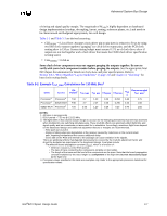
Advanced System Bus Design interference from AGTL+ signals in a particular group to AGTL+ signals in a different group. An example of AGTL+ to non-AGTL+ cross-talk is when CMOS and AGTL+ signals interfere with each other. Table 3-4. Trace Width Space Guidelines Cross-talk Type Intragroup AGTL+ (same group AGTL+) Intergroup AGTL+ (different group AGTL+) AGTL+ to non-AGTL+ Trace Width:Space Ratio 5:10 or 6:12 5:15 or 6:18 5:20 or 6:24 The spacing between the various bus agents causes variations in trunk impedance and stub locations. These variations cause reflections that can cause constructive or destructive interference at the receivers. A reduction of noise may be obtained by a minimum spacing between the agents. Unfortunately, tighter spacing results in reduced component placement options and lower hold margins. Therefore, adjusting the inter-agent spacing may be one way to change the network's noise margin, but mechanical constraints often limit the usefulness of this technique. Always be sure to validate signal quality after making any changes in agent locations or changes to inter-agent spacing. There are six AGTL+ signals that can be driven by more than one agent simultaneously. These signals may require more attention during the layout and validation portions of the design. When a signal is asserted (driven low) by two or more agents on the same clock edge, the two falling edge wave fronts will meet at some point on the bus and can sum to form a negative voltage. The ringback from this negative voltage can easily cross into the overdrive region. The signals are AERR#, BERR#, BINIT#, BNR#, HIT#, and HITM#. This document addresses AGTL+ layout for both 1 and 2-way 133 MHz/100 MHz processor/ Intel® 820 chipset systems. Power distribution and chassis requirements for cooling, connector location, memory location, etc., may constrain the system topology and component placement location; therefore, constraining the board routing. These issues are not directly addressed in this document. Section 1.2, "References" on page 1-2 contains a listing of several documents that address some of these issues. Intel®820 Chipset Design Guide 3-11
-
 1
1 -
2
-
3
-
4
-
5
-
6
-
7
-
8
-
9
-
10
-
11
-
12
-
13
-
14
-
15
-
16
-
17
-
18
-
19
-
20
-
21
-
22
-
23
-
24
-
25
-
26
-
27
-
28
-
29
-
30
-
31
-
32
-
33
-
34
-
35
-
36
-
37
-
38
-
39
-
40
-
41
-
42
-
43
-
44
-
45
-
46
-
47
-
48
-
49
-
50
-
51
-
52
-
53
-
54
-
55
-
56
-
57
-
58
-
59
-
60
-
61
-
62
-
63
-
64
-
65
-
66
-
67
-
68
-
69
-
70
-
71
-
72
-
73
-
74
-
75
-
76
-
77
-
78
-
79
-
80
-
81
-
82
-
83
-
84
-
85
-
86
-
87
-
88
-
89
-
90
-
91
-
92
-
93
-
94
-
95
-
96
-
97
-
98
-
99
-
100
-
101
-
102
-
103
-
104
-
105
-
 106
106 -
 107
107 -
 108
108 -
 109
109 -
 110
110 -
 111
111 -
 112
112 -
 113
113 -
 114
114 -
 115
115 -
 116
116 -
117
-
118
-
119
-
120
-
121
-
122
-
123
-
124
-
125
-
126
-
127
-
128
-
129
-
130
-
131
-
132
-
133
-
134
-
135
-
136
-
137
-
138
-
139
-
140
-
141
-
142
-
143
-
144
-
145
-
146
-
147
-
148
-
149
-
150
-
151
-
152
-
153
-
154
-
155
-
156
-
157
-
158
-
159
-
160
-
161
-
162
-
163
-
164
-
165
-
166
-
167
-
168
-
169
-
170
-
171
-
172
-
173
-
174
-
175
-
176
-
177
-
178
-
179
-
180
-
181
-
182
-
183
-
184
-
185
-
186
-
187
-
188
-
189
-
190
-
191
-
192
-
193
-
194
-
195
-
196
-
197
-
198
-
199
-
200
-
201
-
202
-
203
-
204
-
205
-
206
-
207
-
208
-
209
-
210
-
211
-
212
-
213
-
214
-
215
-
216
-
217
-
218
-
219
-
220
-
221
-
222
-
223
-
224
-
225
-
226
-
227
-
228
-
229
-
230
-
231
-
232
-
233
-
234
-
235
-
236
-
237
-
238
-
239
-
240
-
241
-
242
 |
 |
