Intel VC820 Design Guide - Page 33
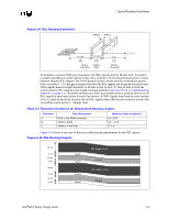
Direct Rambus* Interface, RIMM Diagram
 |
View all Intel VC820 manuals
Add to My Manuals
Save this manual to your list of manuals |
Page 33 highlights
Layout/Routing Guidelines When routing strobes and their associated data lines, trace length mismatch is very important (in addition to noise immunity). The primary benefit of source synchronous strobing is that the data and the strobe arrive at the receiver simultaneously. Thus, a strobe and its associated data signals have very critical length mismatch requirements. With well matched trace lengths (as well as matched impedance), the propagation delay for the strobe, and the propagation delay for the data will be very close. Hence, the strobe and the data arrive at the receiver simultaneously. For some interfaces, the trace length mismatch requirement is less than 0.25 inch. 2.6 Direct Rambus* Interface The Direct Rambus* Channel is a multi-symbol interconnect. Due to the length of the interconnect and the frequency of operation, this bus is designed to allow multiple command and data packets to be present on a signal wire at any given instant. The driving device sends the next data out before the previous data has left the bus. Figure 2-8. RIMM Diagram The nature of the multi-symbol interconnect forces many requirements on the bus design and topology. First and foremost, a drastic reduction in reflected voltage levels is required. The interconnect transmission lines must be terminated at their characteristic impedance, or the reflected voltage resulting from a mismatch in impedance will degrade signal quality. These reflections will reduce noise and timing margins, and reduce the maximum operating frequency of the bus. Potentially, the reflections could create data errors. Due to the tolerances of components such as PCBs, connectors, and termination resistors, there will be some reflected voltage on the interconnect. In this multi-symbol interconnect, timings are pattern dependent due to the reflections interfering with the next transfer. Additionally, coupled noise can greatly affect the performance of high-speed interfaces. Just as in source synchronous designs, the odd and even mode propagation velocity change creates skew between the clock and data or command lines which reduces the maximum operating frequency of the bus. Efforts must be made to significantly decrease crosstalk, as well as the other sources of skew. To achieve these bus requirements, the Direct Rambus* channel is designed to operate as a transmission line; all components, including the individual RDRAMs, are incorporated into the design to create a uniform bus structure that can support up to 33 devices (including the MCH) running at 800 MegaTransfers/second (MT/s). Intel®820 Chipset Design Guide 2-7
-
 1
1 -
2
-
3
-
4
-
5
-
6
-
7
-
8
-
9
-
10
-
11
-
12
-
13
-
14
-
15
-
16
-
17
-
18
-
19
-
20
-
21
-
22
-
23
-
24
-
25
-
26
-
27
-
 28
28 -
 29
29 -
 30
30 -
 31
31 -
 32
32 -
 33
33 -
 34
34 -
 35
35 -
 36
36 -
 37
37 -
 38
38 -
39
-
40
-
41
-
42
-
43
-
44
-
45
-
46
-
47
-
48
-
49
-
50
-
51
-
52
-
53
-
54
-
55
-
56
-
57
-
58
-
59
-
60
-
61
-
62
-
63
-
64
-
65
-
66
-
67
-
68
-
69
-
70
-
71
-
72
-
73
-
74
-
75
-
76
-
77
-
78
-
79
-
80
-
81
-
82
-
83
-
84
-
85
-
86
-
87
-
88
-
89
-
90
-
91
-
92
-
93
-
94
-
95
-
96
-
97
-
98
-
99
-
100
-
101
-
102
-
103
-
104
-
105
-
106
-
107
-
108
-
109
-
110
-
111
-
112
-
113
-
114
-
115
-
116
-
117
-
118
-
119
-
120
-
121
-
122
-
123
-
124
-
125
-
126
-
127
-
128
-
129
-
130
-
131
-
132
-
133
-
134
-
135
-
136
-
137
-
138
-
139
-
140
-
141
-
142
-
143
-
144
-
145
-
146
-
147
-
148
-
149
-
150
-
151
-
152
-
153
-
154
-
155
-
156
-
157
-
158
-
159
-
160
-
161
-
162
-
163
-
164
-
165
-
166
-
167
-
168
-
169
-
170
-
171
-
172
-
173
-
174
-
175
-
176
-
177
-
178
-
179
-
180
-
181
-
182
-
183
-
184
-
185
-
186
-
187
-
188
-
189
-
190
-
191
-
192
-
193
-
194
-
195
-
196
-
197
-
198
-
199
-
200
-
201
-
202
-
203
-
204
-
205
-
206
-
207
-
208
-
209
-
210
-
211
-
212
-
213
-
214
-
215
-
216
-
217
-
218
-
219
-
220
-
221
-
222
-
223
-
224
-
225
-
226
-
227
-
228
-
229
-
230
-
231
-
232
-
233
-
234
-
235
-
236
-
237
-
238
-
239
-
240
-
241
-
242
 |
 |
