Intel VC820 Design Guide - Page 129
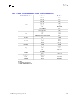
Clocking 4, 4.1 Clock Generation, Table 4-1. Intel, Chipset Platform System Clocks
 |
View all Intel VC820 manuals
Add to My Manuals
Save this manual to your list of manuals |
Page 129 highlights
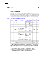
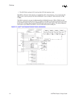
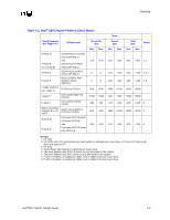
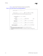
Clocking Clocking 4 4.1 Clock Generation There are two clock generator components required in an Intel® 820 chipset based system. The Direct Rambus* Clock Generator (DRCG) generates clock for the Direct Rambus* interface while the CK133 component generates clocks for the rest of the system. Clock synthesizers that meet the Intel CK98 Clock Specification are suitable for an Intel® 820 chipset based system. The CK133 generates the clocks listed in Table 4-1. Table 4-1. Intel® 820 Chipset Platform System Clocks Number Name on CK133 Used for Routed to Name on Receiver Frequency Voltage 2 Processors CLK 4 CPUCLK[0-3] System Bus Clock MCH HCLKIN 100/133 MHz 2.5V ITP BCLK 3 APIC[0-2] APIC Bus Clock 2 Processors PICCLK 33 MHz ICH APICCLK 2.5V PCI Bus Clock 5 PCI Devices CLK 8 PCI, LPC, FWH Flash PCICLK[1-7,F] BIOS Bus Clock ICH PCICLK 33 MHz FWH Flash BIOS Interface Clock FWH Flash BIOS CLK 3.3V LPC Interface Clock LPC CLK Hub Interface/AGP Bus Clock MCH CLK66 4 3V66[0-3] Hub Interface Clock AGP Bus Clock Unused ICH AGP device/ slot N/A CLK66 CLK N/A 66 MHz 3.3V 2 REF[0-1] Internal ICH Logic ICH Internal Super I/O Logic Super I/O CLK14 Vendor Specific 14 MHz 3.3V 1 48 MHz USB ICH DRCG Reference Clock DRCG 2 CPU_DIV2[0-1] Unused N/A CLK48 REFCLK N/A 48 MHz 50/66 MHz 3.3V 2.5V The CK133 is a mixed voltage component. Some of the output clocks are 3.3V and some of the output clock are 2.5V. As a result, the CK133 device requires both 3.3V and 2.5V. These power supplies should be a clean as possible. Noise in the power delivery system for the clock driver can cause noise on the clock lines. The MCH uses the same clock for hub interface and AGP. It is important that the hub interface/AGP clocks are routed to ensure the skew requirements are met between: • The MCH hub interface/AGP clock and the AGP connector (or device) Intel®820 Chipset Design Guide 4-1
-
 1
1 -
2
-
3
-
4
-
5
-
6
-
7
-
8
-
9
-
10
-
11
-
12
-
13
-
14
-
15
-
16
-
17
-
18
-
19
-
20
-
21
-
22
-
23
-
24
-
25
-
26
-
27
-
28
-
29
-
30
-
31
-
32
-
33
-
34
-
35
-
36
-
37
-
38
-
39
-
40
-
41
-
42
-
43
-
44
-
45
-
46
-
47
-
48
-
49
-
50
-
51
-
52
-
53
-
54
-
55
-
56
-
57
-
58
-
59
-
60
-
61
-
62
-
63
-
64
-
65
-
66
-
67
-
68
-
69
-
70
-
71
-
72
-
73
-
74
-
75
-
76
-
77
-
78
-
79
-
80
-
81
-
82
-
83
-
84
-
85
-
86
-
87
-
88
-
89
-
90
-
91
-
92
-
93
-
94
-
95
-
96
-
97
-
98
-
99
-
100
-
101
-
102
-
103
-
104
-
105
-
106
-
107
-
108
-
109
-
110
-
111
-
112
-
113
-
114
-
115
-
116
-
117
-
118
-
119
-
120
-
121
-
122
-
123
-
 124
124 -
 125
125 -
 126
126 -
 127
127 -
 128
128 -
 129
129 -
 130
130 -
 131
131 -
 132
132 -
 133
133 -
 134
134 -
135
-
136
-
137
-
138
-
139
-
140
-
141
-
142
-
143
-
144
-
145
-
146
-
147
-
148
-
149
-
150
-
151
-
152
-
153
-
154
-
155
-
156
-
157
-
158
-
159
-
160
-
161
-
162
-
163
-
164
-
165
-
166
-
167
-
168
-
169
-
170
-
171
-
172
-
173
-
174
-
175
-
176
-
177
-
178
-
179
-
180
-
181
-
182
-
183
-
184
-
185
-
186
-
187
-
188
-
189
-
190
-
191
-
192
-
193
-
194
-
195
-
196
-
197
-
198
-
199
-
200
-
201
-
202
-
203
-
204
-
205
-
206
-
207
-
208
-
209
-
210
-
211
-
212
-
213
-
214
-
215
-
216
-
217
-
218
-
219
-
220
-
221
-
222
-
223
-
224
-
225
-
226
-
227
-
228
-
229
-
230
-
231
-
232
-
233
-
234
-
235
-
236
-
237
-
238
-
239
-
240
-
241
-
242
 |
 |
