Intel VC820 Design Guide - Page 34
Stackup, 2.6.2 Direct Rambus* Layout Guidelines, 2.6.2.1 RSL Routing
 |
View all Intel VC820 manuals
Add to My Manuals
Save this manual to your list of manuals |
Page 34 highlights
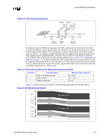
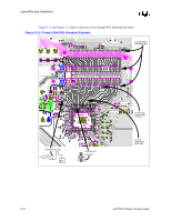
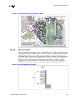
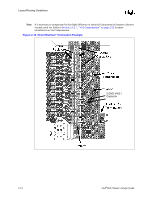
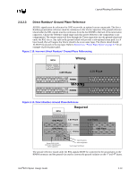
Layout/Routing Guidelines 2.6.1 2.6.2 2.6.2.1 Stackup The perfect matching of transmission line impedance and uniform trace length are essential for the Direct RDRAM interface to work properly. Maintaining 28 Ω (±10%) loaded impedance for every RSL (Direct Rambus* Signaling Level) signal has changed the requirements for trace width and prepreg thickness for the Intel® 820 chipset platform (refer to Section 5.3, "Stackup Requirement" on page 5-1). Achieving a 28 Ω nominal impedance with a traditional 7 mil prepreg requires 28 mil wide traces. These traces are too wide to break out of the two rows of RSL balls on the MCH. To reduce trace width, a 4.5 mil thick prepreg is required. This thinner prepreg allows 18 mil wide traces to meet the 28 Ω (±10%) nominal impedance requirement. Refer to Section 5.3, "Stackup Requirement" on page 5-1 for detailed stackup requirements. Direct Rambus* Layout Guidelines The signals on the Direct Rambus* Channel are broken into three groups: RSL signals, CMOS signals, and Clocking signals. The signal groups are: • RSL Signals - DQA[8:0] - DQB[8:0] - RQ[7:0] • CMOS Signals - CMD (high-speed CMOS signal) - SCK (high-speed CMOS signal) - SIO • Clocking Signals - CTM, CTM# - CFM, CFM# RSL Routing The RSL signals enter the first RIMM on the left side, propagate through the RIMM, and exit on the right. The signal continues through the rest of the existing RIMMs until it is terminated at Vterm. All unpopulated slots must have continuity modules in place to ensure that the signals propagate to the termination. 2-8 Intel®820 Chipset Design Guide
-
 1
1 -
2
-
3
-
4
-
5
-
6
-
7
-
8
-
9
-
10
-
11
-
12
-
13
-
14
-
15
-
16
-
17
-
18
-
19
-
20
-
21
-
22
-
23
-
24
-
25
-
26
-
27
-
28
-
 29
29 -
 30
30 -
 31
31 -
 32
32 -
 33
33 -
 34
34 -
 35
35 -
 36
36 -
 37
37 -
 38
38 -
 39
39 -
40
-
41
-
42
-
43
-
44
-
45
-
46
-
47
-
48
-
49
-
50
-
51
-
52
-
53
-
54
-
55
-
56
-
57
-
58
-
59
-
60
-
61
-
62
-
63
-
64
-
65
-
66
-
67
-
68
-
69
-
70
-
71
-
72
-
73
-
74
-
75
-
76
-
77
-
78
-
79
-
80
-
81
-
82
-
83
-
84
-
85
-
86
-
87
-
88
-
89
-
90
-
91
-
92
-
93
-
94
-
95
-
96
-
97
-
98
-
99
-
100
-
101
-
102
-
103
-
104
-
105
-
106
-
107
-
108
-
109
-
110
-
111
-
112
-
113
-
114
-
115
-
116
-
117
-
118
-
119
-
120
-
121
-
122
-
123
-
124
-
125
-
126
-
127
-
128
-
129
-
130
-
131
-
132
-
133
-
134
-
135
-
136
-
137
-
138
-
139
-
140
-
141
-
142
-
143
-
144
-
145
-
146
-
147
-
148
-
149
-
150
-
151
-
152
-
153
-
154
-
155
-
156
-
157
-
158
-
159
-
160
-
161
-
162
-
163
-
164
-
165
-
166
-
167
-
168
-
169
-
170
-
171
-
172
-
173
-
174
-
175
-
176
-
177
-
178
-
179
-
180
-
181
-
182
-
183
-
184
-
185
-
186
-
187
-
188
-
189
-
190
-
191
-
192
-
193
-
194
-
195
-
196
-
197
-
198
-
199
-
200
-
201
-
202
-
203
-
204
-
205
-
206
-
207
-
208
-
209
-
210
-
211
-
212
-
213
-
214
-
215
-
216
-
217
-
218
-
219
-
220
-
221
-
222
-
223
-
224
-
225
-
226
-
227
-
228
-
229
-
230
-
231
-
232
-
233
-
234
-
235
-
236
-
237
-
238
-
239
-
240
-
241
-
242
 |
 |
