Intel VC820 Design Guide - Page 112
Host Clock Routing, 3.2.4.4 APIC Data Bus Routing, Table 3-5. Host Clock Routing
 |
View all Intel VC820 manuals
Add to My Manuals
Save this manual to your list of manuals |
Page 112 highlights
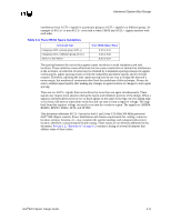
Advanced System Bus Design 3.2.4.3 Host Clock Routing Host clock nets should be routed as point-to-point connections through a series resistor placed as close to the output pins of the clock driver as possible. The value of the series resistor is dependent on the clock driver characteristic impedance. However, a value of 33 Ω is a good starting point. Table 3-5 provides the trace length recommendations for this topology. "H" indicates the length of the host clock trace starting from the clock driver output pin and ending at the SC242 connector BCLK pin. Note that the clock route from the clock driver to the Intel 82820 MCH will require an additional trace length of approximately 4.6" to compensate for the additional propagation delay along the processor host clock path (SC242 connector plus processor cartridge trace). This value of 4.6" assumes a propagation speed of 180 ps/in. Table 3-5. Host Clock Routing Clock Net Trace length Clock driver to SC242 connector Clock driver to Intel 82820 MCH H H + (clock delay from the processor edge to core) + connector delay 3.2.4.4 APIC Data Bus Routing Intel recommends using the in-line topology shown in Figure 3-1 and Figure 3-2 for the APIC Data signals, PICD[1:0]. For dual-processor systems, the network should be dual-end terminated with 330 Ω resistors. The combined routing lengths of L1 plus L2 should be between 0.0" and 12.0". Figure 3-1. PICD[1,0] Uni-Processor Topology 2.5V Intel® 820 Chipset 150 Ω L1 < 8" PICD[1,0] L(1): Z0=60 Ω ±15%. SC242 Figure 3-2. PICD[1,0] Dual-Processor Topology 2.5V 330 Ω L1 Intel® 820 Chipset: ICH SC242 L(1): Z0=60 Ω ±15%. SC242 L2 L1 + L2 < 12" PICD[1,0] 2.5V 330 Ω 3-12 Intel®820 Chipset Design Guide
-
 1
1 -
2
-
3
-
4
-
5
-
6
-
7
-
8
-
9
-
10
-
11
-
12
-
13
-
14
-
15
-
16
-
17
-
18
-
19
-
20
-
21
-
22
-
23
-
24
-
25
-
26
-
27
-
28
-
29
-
30
-
31
-
32
-
33
-
34
-
35
-
36
-
37
-
38
-
39
-
40
-
41
-
42
-
43
-
44
-
45
-
46
-
47
-
48
-
49
-
50
-
51
-
52
-
53
-
54
-
55
-
56
-
57
-
58
-
59
-
60
-
61
-
62
-
63
-
64
-
65
-
66
-
67
-
68
-
69
-
70
-
71
-
72
-
73
-
74
-
75
-
76
-
77
-
78
-
79
-
80
-
81
-
82
-
83
-
84
-
85
-
86
-
87
-
88
-
89
-
90
-
91
-
92
-
93
-
94
-
95
-
96
-
97
-
98
-
99
-
100
-
101
-
102
-
103
-
104
-
105
-
106
-
 107
107 -
 108
108 -
 109
109 -
 110
110 -
 111
111 -
 112
112 -
 113
113 -
 114
114 -
 115
115 -
 116
116 -
 117
117 -
118
-
119
-
120
-
121
-
122
-
123
-
124
-
125
-
126
-
127
-
128
-
129
-
130
-
131
-
132
-
133
-
134
-
135
-
136
-
137
-
138
-
139
-
140
-
141
-
142
-
143
-
144
-
145
-
146
-
147
-
148
-
149
-
150
-
151
-
152
-
153
-
154
-
155
-
156
-
157
-
158
-
159
-
160
-
161
-
162
-
163
-
164
-
165
-
166
-
167
-
168
-
169
-
170
-
171
-
172
-
173
-
174
-
175
-
176
-
177
-
178
-
179
-
180
-
181
-
182
-
183
-
184
-
185
-
186
-
187
-
188
-
189
-
190
-
191
-
192
-
193
-
194
-
195
-
196
-
197
-
198
-
199
-
200
-
201
-
202
-
203
-
204
-
205
-
206
-
207
-
208
-
209
-
210
-
211
-
212
-
213
-
214
-
215
-
216
-
217
-
218
-
219
-
220
-
221
-
222
-
223
-
224
-
225
-
226
-
227
-
228
-
229
-
230
-
231
-
232
-
233
-
234
-
235
-
236
-
237
-
238
-
239
-
240
-
241
-
242
 |
 |
