Intel VC820 Design Guide - Page 50
Table 2-5. Line Matching and Via Compensation Example
 |
View all Intel VC820 manuals
Add to My Manuals
Save this manual to your list of manuals |
Page 50 highlights
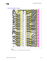
Layout/Routing Guidelines Table 2-5. Line Matching and Via Compensation Example1,2,3,4,5,6,7,8,9,10 Signal Ball on MCH Nominal RSL Length (mils) Package Dimension (mils) Motherboard Trace Length when Routed on Bottom (i.e., Real Via) Min (mils) Max (mils) Motherboard Trace Length when Routed on Top (i.e., Dummy Via) Min (mils) Max (mils) Recommended To Route On DQA0 A13 DQA1 C13 DQA2 A14 DQA3 C14 DQA4 B14 DQA5 C15 DQA6 A15 DQA7 C16 DQA8 A16 DQB0 C7 DQB1 B7 DQB2 C6 DQB3 A6 DQB4 C5 DQB5 A5 DQB6 B5 DQB7 A4 DQB8 C4 RQ0 A7 RQ1 C8 RQ2 A8 RQ3 C9 RQ4 B9 RQ5 A9 RQ6 A10 RQ7 C10 2000 2000 2000 2000 2000 2000 2000 2000 2000 2000 2000 2000 2000 2000 2000 2000 2000 2000 2000 2000 2000 2000 2000 2000 2000 2000 CFM A12 CFM# B12 CTM B11 CTM# A11 2000 2000 2000 2000 138.14 19.11 163.16 39.87 97.54 62.67 186.11 95.70 230.20 39.56 95.83 63.49 153.69 97.33 191.43 152.47 237.71 138.29 179.49 27.12 162.21 5.80 71.70 133.88 122.20 0.00 132.37 64.63 56.06 126.34 Formula A 1851.86 1970.89 1826.84 1950.13 1892.46 1927.33 1803.90 1894.30 1759.81 1950.44 1894.17 1926.51 1836.31 1892.67 1798.57 1837.53 1752.29 1851.71 1810.51 1962.88 1827.79 1984.20 1918.30 1856.12 1867.81 1990.00 1871.86 1990.89 1846.84 1970.13 1912.46 1947.33 1823.90 1914.30 1779.81 1970.44 1914.17 1946.51 1856.31 1912.67 1818.57 1857.53 1772.29 1871.71 1830.51 1982.88 1847.79 2004.20 1938.30 1876.12 1887.81 2010.00 FORMULA C 1906.85 1976.02 1984.76 1913.01 Formula B 1876.86 1995.89 1851.84 1975.13 1917.46 1952.33 1828.90 1919.30 1784.81 1975.44 1919.17 1951.51 1861.31 1917.67 1823.57 1862.53 1777.29 1876.71 1835.51 1987.88 1852.79 2009.20 1943.30 1881.12 1892.81 2015.00 1896.86 2015.89 1871.84 1995.13 1937.46 1972.33 1848.90 1939.30 1804.81 1995.44 1939.17 1971.51 1881.31 1937.67 1843.57 1882.53 1797.29 1896.71 1855.51 2007.88 1872.79 2029.20 1963.30 1901.12 1912.81 2035.00 FORMULA D 1932.37 2001.54 2010.29 1938.53 Top Bottom Top Bottom Top Bottom Top Bottom Top Bottom Top Bottom Top Bottom Top Bottom Top Bottom Top Bottom Top Bottom Top Bottom Top Bottom Bottom Bottom Top Top NOTES: 1. Signals connecting to the "A" side of the RIMM connector (i.e., A1, A2, A3, etc.) should be routed on the top (primary side) of the motherboard; 2. Signals connecting to the "B" side of the RIMM connector should be routed on bottom (solder side). 3. These trace lengths ONLY apply from MCH to the 1st RIMM. All signals must match EXACTLY from RIMM to RIMM. 4. Clock trace lengths include 1.021 trace velocity factor. 5. Formula A min: Motherboard Trace = (Nominal RSL Length - Package Dimension) - 10 mil 6. Formula A max: Motherboard Trace = (Nominal RSL Length - Package Dimension) + 10 mil 7. Formula B min: Motherboard Trace = (Nominal RSL Length - Package Dimension) - 10 mil + 25 mil 8. Formula B max: Motherboard Trace = (Nominal RSL Length - Package Dimension) + 10 mil + 25 mil 9. Formula C: Motherboard Trace = (Nominal RSL Length - Package Dimension) * 1.021 10.Formula D: Motherboard Trace = (Nominal RSL Length - Package Dimension + 25 mil) * 1.021 2-24 Intel®820 Chipset Design Guide
-
 1
1 -
2
-
3
-
4
-
5
-
6
-
7
-
8
-
9
-
10
-
11
-
12
-
13
-
14
-
15
-
16
-
17
-
18
-
19
-
20
-
21
-
22
-
23
-
24
-
25
-
26
-
27
-
28
-
29
-
30
-
31
-
32
-
33
-
34
-
35
-
36
-
37
-
38
-
39
-
40
-
41
-
42
-
43
-
44
-
 45
45 -
 46
46 -
 47
47 -
 48
48 -
 49
49 -
 50
50 -
 51
51 -
 52
52 -
 53
53 -
 54
54 -
 55
55 -
56
-
57
-
58
-
59
-
60
-
61
-
62
-
63
-
64
-
65
-
66
-
67
-
68
-
69
-
70
-
71
-
72
-
73
-
74
-
75
-
76
-
77
-
78
-
79
-
80
-
81
-
82
-
83
-
84
-
85
-
86
-
87
-
88
-
89
-
90
-
91
-
92
-
93
-
94
-
95
-
96
-
97
-
98
-
99
-
100
-
101
-
102
-
103
-
104
-
105
-
106
-
107
-
108
-
109
-
110
-
111
-
112
-
113
-
114
-
115
-
116
-
117
-
118
-
119
-
120
-
121
-
122
-
123
-
124
-
125
-
126
-
127
-
128
-
129
-
130
-
131
-
132
-
133
-
134
-
135
-
136
-
137
-
138
-
139
-
140
-
141
-
142
-
143
-
144
-
145
-
146
-
147
-
148
-
149
-
150
-
151
-
152
-
153
-
154
-
155
-
156
-
157
-
158
-
159
-
160
-
161
-
162
-
163
-
164
-
165
-
166
-
167
-
168
-
169
-
170
-
171
-
172
-
173
-
174
-
175
-
176
-
177
-
178
-
179
-
180
-
181
-
182
-
183
-
184
-
185
-
186
-
187
-
188
-
189
-
190
-
191
-
192
-
193
-
194
-
195
-
196
-
197
-
198
-
199
-
200
-
201
-
202
-
203
-
204
-
205
-
206
-
207
-
208
-
209
-
210
-
211
-
212
-
213
-
214
-
215
-
216
-
217
-
218
-
219
-
220
-
221
-
222
-
223
-
224
-
225
-
226
-
227
-
228
-
229
-
230
-
231
-
232
-
233
-
234
-
235
-
236
-
237
-
238
-
239
-
240
-
241
-
242
 |
 |
