Intel VC820 Design Guide - Page 131
Table 4-2. Intel, Chipset Platform Clock Skews, Clock Symbols, See Relationship, Notes
 |
View all Intel VC820 manuals
Add to My Manuals
Save this manual to your list of manuals |
Page 131 highlights
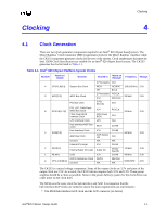
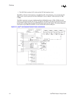
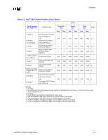
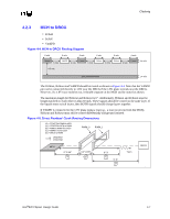
Clocking Table 4-2. Intel® 820 Chipset Platform Clock Skews Skew Clock Symbols See Figure 4-1 Relationship Pin-to-Pin (ps) Board (ps) Total (ps) Notes Min Max Min Max Min Max A leads C, A leads E (or C leads E) SC242 HCLK to SC242 HCLK (DP ONLY) And SC242 HCLK to MCH HCLK (DP ONLY) -175 A leads E SC242 HCLK to MCH HCLK (UP ONLY) 0 P leads F MCH CLK66 to AGP graphics device 0 AGPCLK L leads another L PCICLK to PCICLK (or L leads H) -500 I leads H ICH CLK66 leads ICH PCICLK +1500 F leads I ICH CLK66 to MCH CLK66 -250 Worst case skew between H, L, M and N Worst case FWHCLK, LPCCLK, PCICLK -500 B leads D, B leads G Processor PICCLK leads Processor PICCLK And Processor PICCLK leads ICH APICCLK -250 +175 0 0 +500 +4000 250 +500 +250 -125 -125 -125 -1500 -500 -125 -1500 -125 +125 +125 +125 +1500 +500 +125 +1500 +125 -300 -125 -125 -2000 +1000 -375 -2000 -375 +300 1, 7 +125 2, 3, 7 +125 4, 8 +2000 +4500 +375 8 +2000 5 +375 6 NOTES: 1. DP Only 2. UP: MCH and CPU clock drivers are tied together to eliminate pin-to-pin skew. -175 and +175 pin-to-pin skew only apply to DP. 3. UP Only 4. Clock drivers tied together to eliminate pin-to-pin skew. 5. The skew between any PCICLK clocks on any two inputs in the system. 6. The skew between any APIC clocks on any two inputs in the system. 7. If SSC is enabled, an additional ±40ps must is added to the pin-to-pin skew 8. If SSC is enabled, an additional ±60ps must is added to the pin-to-pin skew Intel®820 Chipset Design Guide 4-3
-
 1
1 -
2
-
3
-
4
-
5
-
6
-
7
-
8
-
9
-
10
-
11
-
12
-
13
-
14
-
15
-
16
-
17
-
18
-
19
-
20
-
21
-
22
-
23
-
24
-
25
-
26
-
27
-
28
-
29
-
30
-
31
-
32
-
33
-
34
-
35
-
36
-
37
-
38
-
39
-
40
-
41
-
42
-
43
-
44
-
45
-
46
-
47
-
48
-
49
-
50
-
51
-
52
-
53
-
54
-
55
-
56
-
57
-
58
-
59
-
60
-
61
-
62
-
63
-
64
-
65
-
66
-
67
-
68
-
69
-
70
-
71
-
72
-
73
-
74
-
75
-
76
-
77
-
78
-
79
-
80
-
81
-
82
-
83
-
84
-
85
-
86
-
87
-
88
-
89
-
90
-
91
-
92
-
93
-
94
-
95
-
96
-
97
-
98
-
99
-
100
-
101
-
102
-
103
-
104
-
105
-
106
-
107
-
108
-
109
-
110
-
111
-
112
-
113
-
114
-
115
-
116
-
117
-
118
-
119
-
120
-
121
-
122
-
123
-
124
-
125
-
 126
126 -
 127
127 -
 128
128 -
 129
129 -
 130
130 -
 131
131 -
 132
132 -
 133
133 -
 134
134 -
 135
135 -
 136
136 -
137
-
138
-
139
-
140
-
141
-
142
-
143
-
144
-
145
-
146
-
147
-
148
-
149
-
150
-
151
-
152
-
153
-
154
-
155
-
156
-
157
-
158
-
159
-
160
-
161
-
162
-
163
-
164
-
165
-
166
-
167
-
168
-
169
-
170
-
171
-
172
-
173
-
174
-
175
-
176
-
177
-
178
-
179
-
180
-
181
-
182
-
183
-
184
-
185
-
186
-
187
-
188
-
189
-
190
-
191
-
192
-
193
-
194
-
195
-
196
-
197
-
198
-
199
-
200
-
201
-
202
-
203
-
204
-
205
-
206
-
207
-
208
-
209
-
210
-
211
-
212
-
213
-
214
-
215
-
216
-
217
-
218
-
219
-
220
-
221
-
222
-
223
-
224
-
225
-
226
-
227
-
228
-
229
-
230
-
231
-
232
-
233
-
234
-
235
-
236
-
237
-
238
-
239
-
240
-
241
-
242
 |
 |
