Intel VC820 Design Guide - Page 114
Validation, 3.2.6.1 Measurements, 3.2.6.2 Flight Time Simulation
 |
View all Intel VC820 manuals
Add to My Manuals
Save this manual to your list of manuals |
Page 114 highlights
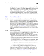
Advanced System Bus Design 3.2.6 Validation Build systems and validate the design and simulation assumptions. 3.2.6.1 Measurements Note that the AGTL+ specification for signal quality is at the pad of the component. The expected method of determining the signal quality is to run analog simulations for the pin and the pad. Then correlate the simulations at the pin against actual system measurements at the pin. Good correlation at the pin leads to confidence that the simulation at the pad is accurate. Controlling the temperature and voltage to correspond to the I/O buffer model extremes should enhance the correlation between simulations and the actual system. 3.2.6.2 Flight Time Simulation As defined in Section 3.1, "Terminology and Definitions" on page 3-1, flight time is the time difference between a signal crossing VREF at the input pin of the receiver, and the output pin of the driver crossing VREF were it driving a test load. The timings in the tables and topologies discussed in this guideline assume the actual system load is 50 Ω and is equal to the test load. While the DC loading of the AGTL+ bus in a DP mode is closer to 25 Ω, AC loading is approximately 29 Ω since the driver effectively "sees" a 56 Ω termination resistor in parallel with a 60 Ω transmission line on the cartridge. Figure 3-3. Test Load vs. Actual System Load CLK I/O Buffer Vcc Driver Pad D SETQ VTT RTEST Test Load Driver Pin CLR Q TREF TCO CLK I/O Buffer Vcc Driver Pad D SETQ CLR Q Actual System Load VTT RTT Receiver Pin TFLIGHTSYSTEM Figure 3-3 above shows the different configurations for TCO testing and flight time simulation. The flip-flop represents the logic input and driver stage of a typical AGTL+ I/O buffer. TCO timings are specified at the driver pin output. TFLIGHT-SYSTEM is usually reported by a simulation tool as the time from the driver pad starting its transition to the time when the receiver's input pin sees a valid data input. Since both timing numbers (TCO and TFLIGHT-SYSTEM) include propagation time from the pad to the pin, it is necessary to subtract this time (TREF) from the reported flight time to avoid 3-14 Intel®820 Chipset Design Guide
-
 1
1 -
2
-
3
-
4
-
5
-
6
-
7
-
8
-
9
-
10
-
11
-
12
-
13
-
14
-
15
-
16
-
17
-
18
-
19
-
20
-
21
-
22
-
23
-
24
-
25
-
26
-
27
-
28
-
29
-
30
-
31
-
32
-
33
-
34
-
35
-
36
-
37
-
38
-
39
-
40
-
41
-
42
-
43
-
44
-
45
-
46
-
47
-
48
-
49
-
50
-
51
-
52
-
53
-
54
-
55
-
56
-
57
-
58
-
59
-
60
-
61
-
62
-
63
-
64
-
65
-
66
-
67
-
68
-
69
-
70
-
71
-
72
-
73
-
74
-
75
-
76
-
77
-
78
-
79
-
80
-
81
-
82
-
83
-
84
-
85
-
86
-
87
-
88
-
89
-
90
-
91
-
92
-
93
-
94
-
95
-
96
-
97
-
98
-
99
-
100
-
101
-
102
-
103
-
104
-
105
-
106
-
107
-
108
-
 109
109 -
 110
110 -
 111
111 -
 112
112 -
 113
113 -
 114
114 -
 115
115 -
 116
116 -
 117
117 -
 118
118 -
 119
119 -
120
-
121
-
122
-
123
-
124
-
125
-
126
-
127
-
128
-
129
-
130
-
131
-
132
-
133
-
134
-
135
-
136
-
137
-
138
-
139
-
140
-
141
-
142
-
143
-
144
-
145
-
146
-
147
-
148
-
149
-
150
-
151
-
152
-
153
-
154
-
155
-
156
-
157
-
158
-
159
-
160
-
161
-
162
-
163
-
164
-
165
-
166
-
167
-
168
-
169
-
170
-
171
-
172
-
173
-
174
-
175
-
176
-
177
-
178
-
179
-
180
-
181
-
182
-
183
-
184
-
185
-
186
-
187
-
188
-
189
-
190
-
191
-
192
-
193
-
194
-
195
-
196
-
197
-
198
-
199
-
200
-
201
-
202
-
203
-
204
-
205
-
206
-
207
-
208
-
209
-
210
-
211
-
212
-
213
-
214
-
215
-
216
-
217
-
218
-
219
-
220
-
221
-
222
-
223
-
224
-
225
-
226
-
227
-
228
-
229
-
230
-
231
-
232
-
233
-
234
-
235
-
236
-
237
-
238
-
239
-
240
-
241
-
242
 |
 |
