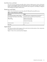
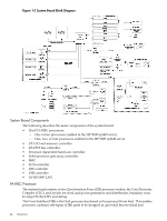
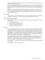
HP rp3440 User Service Guide, Sixth Edition - HP 9000 rp3410/rp3440 - Page 26
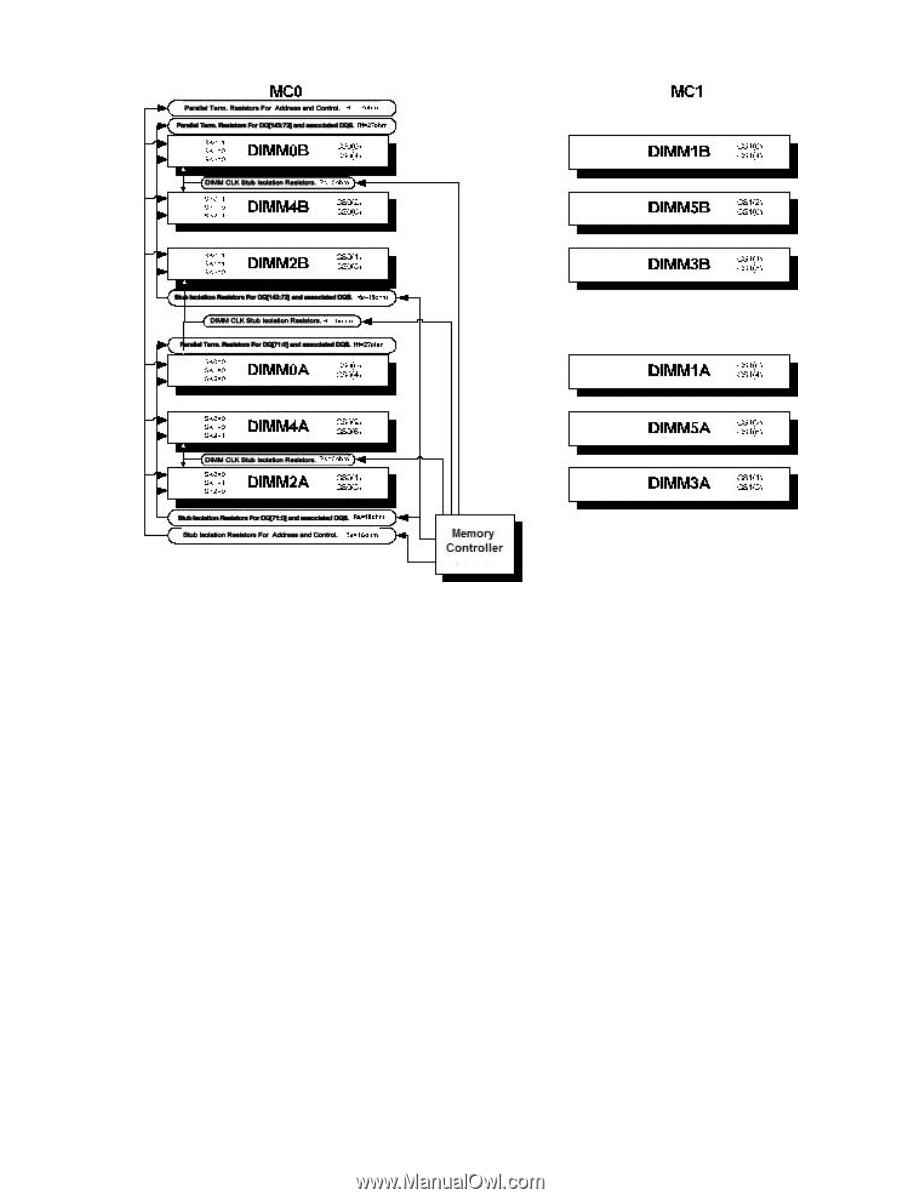
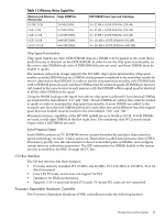
Memory Architecture, DIMMs, Memory Array Capacities, Memory Block Diagram
 |
View all HP rp3440 manuals
Add to My Manuals
Save this manual to your list of manuals |
Page 26 highlights
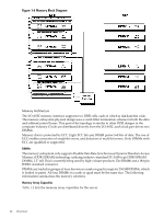
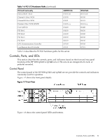
Figure 1-6 Memory Block Diagram Memory Architecture The I/O ASIC memory interface supports two DDR cells, each of which is 144 data bits wide. The memory subsystem physical design uses a comb-filter termination scheme for both the data and address/control buses. This part of the topology is similar to other DDR designs in the computer industry. Clocks are distributed directly from the I/O ASIC; each clock pair drives two DIMMs. Memory data is protected by ECC. Eight ECC bits per DIMM protect 64 bits of data. The use of ECC enables correction of single-bit errors, and detection of multi-bit errors. Only DIMMs with ECC are qualified or supported. DIMMs The memory subsystem only supports Double Data Rate Synchronous Dynamic Random Access Memory (DDR SDRAM) technology utilizing industry-standard PC-1600 type DDR SDRAM DIMMs, 1.2" tall. This is currently being used by high-volume products. The DIMMs use a 184-pin JEDEC standard connector. DIMMs are loaded in groups of four, known as a rank or quad (except for 256 MB DIMMs, which is loaded in pairs). All four DIMMs in a rank or quad must be the same size. The following information summarizes the memory solutions. Memory Array Capacities Table 1-2 lists the memory array capacities for the server. 26 Overview
-
 1
1 -
2
-
3
-
4
-
5
-
6
-
7
-
8
-
9
-
10
-
11
-
12
-
13
-
14
-
15
-
16
-
17
-
18
-
19
-
20
-
 21
21 -
 22
22 -
 23
23 -
 24
24 -
 25
25 -
 26
26 -
 27
27 -
 28
28 -
 29
29 -
 30
30 -
 31
31 -
32
-
33
-
34
-
35
-
36
-
37
-
38
-
39
-
40
-
41
-
42
-
43
-
44
-
45
-
46
-
47
-
48
-
49
-
50
-
51
-
52
-
53
-
54
-
55
-
56
-
57
-
58
-
59
-
60
-
61
-
62
-
63
-
64
-
65
-
66
-
67
-
68
-
69
-
70
-
71
-
72
-
73
-
74
-
75
-
76
-
77
-
78
-
79
-
80
-
81
-
82
-
83
-
84
-
85
-
86
-
87
-
88
-
89
-
90
-
91
-
92
-
93
-
94
-
95
-
96
-
97
-
98
-
99
-
100
-
101
-
102
-
103
-
104
-
105
-
106
-
107
-
108
-
109
-
110
-
111
-
112
-
113
-
114
-
115
-
116
-
117
-
118
-
119
-
120
-
121
-
122
-
123
-
124
-
125
-
126
-
127
-
128
-
129
-
130
-
131
-
132
-
133
-
134
-
135
-
136
-
137
-
138
-
139
-
140
-
141
-
142
-
143
-
144
-
145
-
146
-
147
-
148
-
149
-
150
-
151
-
152
-
153
-
154
-
155
-
156
-
157
-
158
-
159
-
160
-
161
-
162
-
163
-
164
-
165
-
166
-
167
-
168
-
169
-
170
-
171
-
172
-
173
-
174
-
175
-
176
-
177
-
178
-
179
-
180
-
181
-
182
-
183
-
184
-
185
-
186
-
187
-
188
-
189
-
190
-
191
-
192
-
193
-
194
-
195
-
196
-
197
-
198
-
199
-
200
-
201
-
202
-
203
-
204
-
205
-
206
-
207
-
208
-
209
-
210
 |
 |