Intel 925 Data Sheet - Page 109
Host-PCI Express* Graphics Bridge Registers (D1:F0
 |
UPC - 683728067724
View all Intel 925 manuals
Add to My Manuals
Save this manual to your list of manuals |
Page 109 highlights
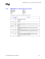
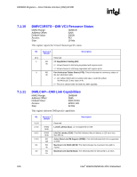
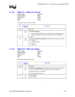
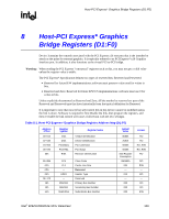
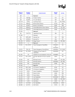
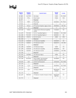
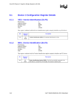
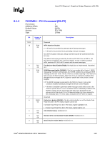
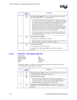
Host-PCI Express* Graphics Bridge Registers (D1:F0) R 8 Host-PCI Express* Graphics Bridge Registers (D1:F0) Device 1contains the controls associated with the PCI Express x16 root port that is the intended to attach as the point for external graphics. It is typically referred to as PCI Express* x16 Graphics Interface port. In addition, it also functions as the virtual PCI-to-PCI bridge. Warning: When reading the PCI Express "conceptual" registers such as this, you may not get a valid value unless the register value is stable. The PCI Express* Specification defines two types of reserved bits: Reserved and Preserved: • Reserved for future R/W implementations; software must preserve value read for writes to bits. • Reserved and Zero: Reserved for future R/WC/S implementations; software must use 0 for writes to bits. Unless explicitly documented as Reserved and Zero, all bits marked as reserved are part of the Reserved and Preserved type that have historically been the typical definition for Reserved. It is important to note that most (if not all) control bits in this device cannot be modified unless the link is down. Software is required to first Disable the link, then program the registers, and then re-enable the link (which will cause a full-retrain with the new settings). Table 8-1. Host-PCI Express* Graphics Bridge Register Address Map (D1:F0) Address Offset 00-01h 02-03h 04-05h 06-07h 08h 09-0Bh 0Ch 0Dh 0Eh 0F-17h 18h 19h 1Ah Register Symbol VID1 DID1 PCICMD1 PCISTS1 RID1 CC1 CL1 - HDR1 - PBUSN1 SBUSN1 SUBUSN1 Register Name Vendor Identification Device Identification PCI Command PCI Status Revision Identification Class Code Cache Line Size Reserved Header Type Reserved Primary Bus Number Secondary Bus Number Subordinate Bus Number Default Value 8086h 2581h 0000h 0000h See Register Description 060400h 00h - 01h - 00h 00h 00h Access RO RO RO, R/W RO, R/W RO RO R/W - RO - RO RO R/W Intel® 82925X/82925XE MCH Datasheet 109
-
 1
1 -
2
-
3
-
4
-
5
-
6
-
7
-
8
-
9
-
10
-
11
-
12
-
13
-
14
-
15
-
16
-
17
-
18
-
19
-
20
-
21
-
22
-
23
-
24
-
25
-
26
-
27
-
28
-
29
-
30
-
31
-
32
-
33
-
34
-
35
-
36
-
37
-
38
-
39
-
40
-
41
-
42
-
43
-
44
-
45
-
46
-
47
-
48
-
49
-
50
-
51
-
52
-
53
-
54
-
55
-
56
-
57
-
58
-
59
-
60
-
61
-
62
-
63
-
64
-
65
-
66
-
67
-
68
-
69
-
70
-
71
-
72
-
73
-
74
-
75
-
76
-
77
-
78
-
79
-
80
-
81
-
82
-
83
-
84
-
85
-
86
-
87
-
88
-
89
-
90
-
91
-
92
-
93
-
94
-
95
-
96
-
97
-
98
-
99
-
100
-
101
-
102
-
103
-
 104
104 -
 105
105 -
 106
106 -
 107
107 -
 108
108 -
 109
109 -
 110
110 -
 111
111 -
 112
112 -
 113
113 -
 114
114 -
115
-
116
-
117
-
118
-
119
-
120
-
121
-
122
-
123
-
124
-
125
-
126
-
127
-
128
-
129
-
130
-
131
-
132
-
133
-
134
-
135
-
136
-
137
-
138
-
139
-
140
-
141
-
142
-
143
-
144
-
145
-
146
-
147
-
148
-
149
-
150
-
151
-
152
-
153
-
154
-
155
-
156
-
157
-
158
-
159
-
160
-
161
-
162
-
163
-
164
-
165
-
166
-
167
-
168
-
169
-
170
-
171
-
172
-
173
-
174
-
175
-
176
-
177
-
178
-
179
-
180
-
181
-
182
-
183
-
184
-
185
-
186
-
187
-
188
-
189
-
190
-
191
-
192
-
193
-
194
-
195
-
196
-
197
-
198
-
199
-
200
-
201
-
202
-
203
-
204
-
205
-
206
-
207
-
208
-
209
-
210
-
211
-
212
-
213
-
214
-
215
-
216
-
217
-
218
-
219
-
220
-
221
-
222
-
223
-
224
-
225
-
226
-
227
-
228
-
229
-
230
-
231
-
232
-
233
-
234
-
235
-
236
-
237
-
238
-
239
-
240
-
241
-
242
 |
 |