Intel 925 Data Sheet - Page 16
Reference Documents, MCH Overview, Host Interface - lga775
 |
UPC - 683728067724
View all Intel 925 manuals
Add to My Manuals
Save this manual to your list of manuals |
Page 16 highlights
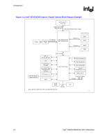
Introduction R 1.2 1.3 1.3.1 16 Reference Documents Document Title Intel® 925X/925XE Express Chipset Thermal Design Guide Intel® I/O Controller Hub 6 (ICH6) Family Datasheet Advanced Configuration and Power Interface Specification, Version 2.0 Advanced Configuration and Power Interface Specification, Version 1.0b The PCI Local Bus Specification, Version 2.3 PCI Express* Specification, Version 1.0a Document Number/Location http://intel.com/design/chipsets/ designex/301466.htm http://intel.com/design/chipsets/ datashts/301473.htm http://www.acpi.info/ http://www.acpi.info/ http://www.pcisig.com/specificat ions http://www.pcisig.com/specificat ions MCH Overview The MCH connects to the processor as shown in Figure 1-1. A major role of the MCH in a system is to manage the flow of information between its interfaces: the processor interface (FSB), the System Memory interface (DRAM controller), the external graphics interface via PCI Express, and the I/O Controller Hub through the DMI interface. This includes arbitrating between the interfaces when each initiates transactions. The processor interface supports the Pentium 4 processor subset of the Extended Mode of the Scalable Bus Protocol. The MCH supports one or two channels of DDR2 SDRAM. The MCH also supports the new PCI Express based external graphics attach. Thus, the 925X/925XE Express chipset is not compatible with AGP (1X, 2X, 4X, or 8X). To increase system performance, the MCH incorporates several queues and a write cache. The MCH also contains advanced desktop power management logic. Host Interface The MCH is optimized for the Pentium 4 processors in the LGA775 socket. The 82925X MCH supports a FSB frequency of 200 MHz (800 MT/s) using a scalable FSB. The 82925XE MCH supports a FSB frequency of 266 MHz (1066 MT/s). The MCH supports the Pentium 4 processor subset of the Extended Mode Scaleable Bus Protocol. The primary enhancements over the Compatible Mode P6 bus protocol are: Source synchronous double-pumped (2) Address and Source synchronous quad-pumped (4x) Data. The MCH supports 32-bit host addressing, decoding up to 4 GB of the processor's memory address space. Host-initiated I/O cycles are decoded to PCI Express, DMI, or the MCH configuration space. Host-initiated memory cycles are decoded to PCI Express, DMI, or system memory. PCI Express device accesses to non-cacheable system memory are not snooped on the host bus. Memory accesses initiated from PCI Express using PCI semantics and from DMI to system memory will be snooped on the host bus. Intel® 82925X/82925XE MCH Datasheet
-
 1
1 -
2
-
3
-
4
-
5
-
6
-
7
-
8
-
9
-
10
-
 11
11 -
 12
12 -
 13
13 -
 14
14 -
 15
15 -
 16
16 -
 17
17 -
 18
18 -
 19
19 -
 20
20 -
 21
21 -
22
-
23
-
24
-
25
-
26
-
27
-
28
-
29
-
30
-
31
-
32
-
33
-
34
-
35
-
36
-
37
-
38
-
39
-
40
-
41
-
42
-
43
-
44
-
45
-
46
-
47
-
48
-
49
-
50
-
51
-
52
-
53
-
54
-
55
-
56
-
57
-
58
-
59
-
60
-
61
-
62
-
63
-
64
-
65
-
66
-
67
-
68
-
69
-
70
-
71
-
72
-
73
-
74
-
75
-
76
-
77
-
78
-
79
-
80
-
81
-
82
-
83
-
84
-
85
-
86
-
87
-
88
-
89
-
90
-
91
-
92
-
93
-
94
-
95
-
96
-
97
-
98
-
99
-
100
-
101
-
102
-
103
-
104
-
105
-
106
-
107
-
108
-
109
-
110
-
111
-
112
-
113
-
114
-
115
-
116
-
117
-
118
-
119
-
120
-
121
-
122
-
123
-
124
-
125
-
126
-
127
-
128
-
129
-
130
-
131
-
132
-
133
-
134
-
135
-
136
-
137
-
138
-
139
-
140
-
141
-
142
-
143
-
144
-
145
-
146
-
147
-
148
-
149
-
150
-
151
-
152
-
153
-
154
-
155
-
156
-
157
-
158
-
159
-
160
-
161
-
162
-
163
-
164
-
165
-
166
-
167
-
168
-
169
-
170
-
171
-
172
-
173
-
174
-
175
-
176
-
177
-
178
-
179
-
180
-
181
-
182
-
183
-
184
-
185
-
186
-
187
-
188
-
189
-
190
-
191
-
192
-
193
-
194
-
195
-
196
-
197
-
198
-
199
-
200
-
201
-
202
-
203
-
204
-
205
-
206
-
207
-
208
-
209
-
210
-
211
-
212
-
213
-
214
-
215
-
216
-
217
-
218
-
219
-
220
-
221
-
222
-
223
-
224
-
225
-
226
-
227
-
228
-
229
-
230
-
231
-
232
-
233
-
234
-
235
-
236
-
237
-
238
-
239
-
240
-
241
-
242
 |
 |