Intel 925 Data Sheet - Page 155
LE1A-Link Entry 1 Address D1:F0, PEGSSTS-PCI Express*-G Sequence Status D1:F0
 |
UPC - 683728067724
View all Intel 925 manuals
Add to My Manuals
Save this manual to your list of manuals |
Page 155 highlights
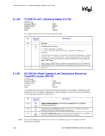
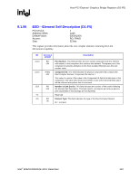
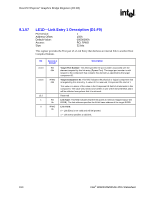
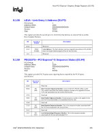
Host-PCI Express* Graphics Bridge Registers (D1:F0) R 8.1.58 LE1A-Link Entry 1 Address (D1:F0) PCI Device: Address Offset: Default Value: Access: Size: 1 158h 0000000000000000h R/WO 64 bits This register provides the second part of a Link Entry that declares an internal link to another Root Complex Element. Bit 63:32 31:12 11:0 Access & Default R/WO 0 0000h Description Reserved Link Address: This field indicates memory-mapped base address of the RCRB that is the target element (Egress Port) for this link entry. Reserved 8.1.59 PEGSSTS-PCI Express*-G Sequence Status (D1:F0) PCI Device: Address Offset: Default Value: Access: Size: 1 218h 0000000000000FFFh RO 64 bits This register provides PCI Express status reporting that is required by the PCI Express specification. Bit 63:60 59:48 47:44 43:32 31:28 27:16 15:12 11:0 Access & Default Description RO 000h RO 000h RO 000h RO FFFh Reserved Next Transmit Sequence Number: Value of the NXT_TRANS_SEQ counter. This counter represents the transmit Sequence number to be applied to the next TLP to be transmitted onto the Link for the first time. Reserved Next Packet Sequence Number: Packet sequence number to be applied to the next TLP to be transmitted or re-transmitted onto the Link. Reserved Next Receive Sequence Number: This is the sequence number associated with the TLP that is expected to be received next. Reserved Last Acknowledged Sequence Number: This is the sequence number associated with the last acknowledged TLP. § Intel® 82925X/82925XE MCH Datasheet 155
-
 1
1 -
2
-
3
-
4
-
5
-
6
-
7
-
8
-
9
-
10
-
11
-
12
-
13
-
14
-
15
-
16
-
17
-
18
-
19
-
20
-
21
-
22
-
23
-
24
-
25
-
26
-
27
-
28
-
29
-
30
-
31
-
32
-
33
-
34
-
35
-
36
-
37
-
38
-
39
-
40
-
41
-
42
-
43
-
44
-
45
-
46
-
47
-
48
-
49
-
50
-
51
-
52
-
53
-
54
-
55
-
56
-
57
-
58
-
59
-
60
-
61
-
62
-
63
-
64
-
65
-
66
-
67
-
68
-
69
-
70
-
71
-
72
-
73
-
74
-
75
-
76
-
77
-
78
-
79
-
80
-
81
-
82
-
83
-
84
-
85
-
86
-
87
-
88
-
89
-
90
-
91
-
92
-
93
-
94
-
95
-
96
-
97
-
98
-
99
-
100
-
101
-
102
-
103
-
104
-
105
-
106
-
107
-
108
-
109
-
110
-
111
-
112
-
113
-
114
-
115
-
116
-
117
-
118
-
119
-
120
-
121
-
122
-
123
-
124
-
125
-
126
-
127
-
128
-
129
-
130
-
131
-
132
-
133
-
134
-
135
-
136
-
137
-
138
-
139
-
140
-
141
-
142
-
143
-
144
-
145
-
146
-
147
-
148
-
149
-
 150
150 -
 151
151 -
 152
152 -
 153
153 -
 154
154 -
 155
155 -
 156
156 -
 157
157 -
 158
158 -
 159
159 -
 160
160 -
161
-
162
-
163
-
164
-
165
-
166
-
167
-
168
-
169
-
170
-
171
-
172
-
173
-
174
-
175
-
176
-
177
-
178
-
179
-
180
-
181
-
182
-
183
-
184
-
185
-
186
-
187
-
188
-
189
-
190
-
191
-
192
-
193
-
194
-
195
-
196
-
197
-
198
-
199
-
200
-
201
-
202
-
203
-
204
-
205
-
206
-
207
-
208
-
209
-
210
-
211
-
212
-
213
-
214
-
215
-
216
-
217
-
218
-
219
-
220
-
221
-
222
-
223
-
224
-
225
-
226
-
227
-
228
-
229
-
230
-
231
-
232
-
233
-
234
-
235
-
236
-
237
-
238
-
239
-
240
-
241
-
242
 |
 |