Intel 925 Data Sheet - Page 57
DMIBAR-Root Complex Register Range Base Address, D0:F0
 |
UPC - 683728067724
View all Intel 925 manuals
Add to My Manuals
Save this manual to your list of manuals |
Page 57 highlights
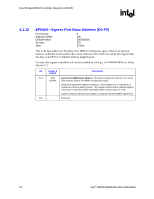
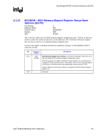
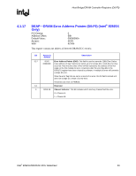
Host Bridge/DRAM Controller Registers (D0:F0) R 4.1.15 DMIBAR-Root Complex Register Range Base Address (D0:F0) PCI Device: Address Offset: Default Value: Access: Size: 0 4Ch 00000000h R/W 32 bits This is the base address for the Root Complex configuration space. This window of addresses contains the Root Complex Register set for the PCI Express hierarchy associated with the MCH. There is no physical memory within this 4-KB window that can be addressed. The 4 KB that is reserved by this register does not alias to any PCI 2.3 compliant memory mapped space. On reset, this register is disabled and must be enabled by writing a 1 to the DMIBAREN [Dev 0, offset 54h, bit 29]. | Bit Access & Default Description 31:12 11:0 R/W 0000 0h DMI Base Address: This field corresponds to bits 31 to 12 of the base address DMI configuration space. BIOS will program this register resulting in a base address for a 4-KB block of contiguous memory address space. This register ensures that a naturally aligned 4-KB space is allocated within total addressable memory space of 4 GB. System software uses this base address to program the DMI register set. Reserved Intel® 82925X/82925XE MCH Datasheet 57
-
 1
1 -
2
-
3
-
4
-
5
-
6
-
7
-
8
-
9
-
10
-
11
-
12
-
13
-
14
-
15
-
16
-
17
-
18
-
19
-
20
-
21
-
22
-
23
-
24
-
25
-
26
-
27
-
28
-
29
-
30
-
31
-
32
-
33
-
34
-
35
-
36
-
37
-
38
-
39
-
40
-
41
-
42
-
43
-
44
-
45
-
46
-
47
-
48
-
49
-
50
-
51
-
 52
52 -
 53
53 -
 54
54 -
 55
55 -
 56
56 -
 57
57 -
 58
58 -
 59
59 -
 60
60 -
 61
61 -
 62
62 -
63
-
64
-
65
-
66
-
67
-
68
-
69
-
70
-
71
-
72
-
73
-
74
-
75
-
76
-
77
-
78
-
79
-
80
-
81
-
82
-
83
-
84
-
85
-
86
-
87
-
88
-
89
-
90
-
91
-
92
-
93
-
94
-
95
-
96
-
97
-
98
-
99
-
100
-
101
-
102
-
103
-
104
-
105
-
106
-
107
-
108
-
109
-
110
-
111
-
112
-
113
-
114
-
115
-
116
-
117
-
118
-
119
-
120
-
121
-
122
-
123
-
124
-
125
-
126
-
127
-
128
-
129
-
130
-
131
-
132
-
133
-
134
-
135
-
136
-
137
-
138
-
139
-
140
-
141
-
142
-
143
-
144
-
145
-
146
-
147
-
148
-
149
-
150
-
151
-
152
-
153
-
154
-
155
-
156
-
157
-
158
-
159
-
160
-
161
-
162
-
163
-
164
-
165
-
166
-
167
-
168
-
169
-
170
-
171
-
172
-
173
-
174
-
175
-
176
-
177
-
178
-
179
-
180
-
181
-
182
-
183
-
184
-
185
-
186
-
187
-
188
-
189
-
190
-
191
-
192
-
193
-
194
-
195
-
196
-
197
-
198
-
199
-
200
-
201
-
202
-
203
-
204
-
205
-
206
-
207
-
208
-
209
-
210
-
211
-
212
-
213
-
214
-
215
-
216
-
217
-
218
-
219
-
220
-
221
-
222
-
223
-
224
-
225
-
226
-
227
-
228
-
229
-
230
-
231
-
232
-
233
-
234
-
235
-
236
-
237
-
238
-
239
-
240
-
241
-
242
 |
 |