Intel 925 Data Sheet - Page 132
MC-Message Control D1:F0
 |
UPC - 683728067724
View all Intel 925 manuals
Add to My Manuals
Save this manual to your list of manuals |
Page 132 highlights
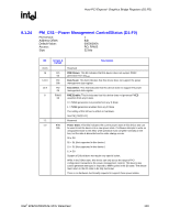
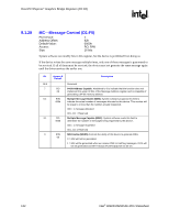
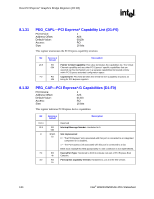
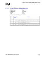
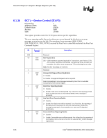
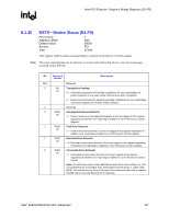
Host-PCI Express* Graphics Bridge Registers (D1:F0) R 8.1.28 MC-Message Control (D1:F0) PCI Device: Address Offset: Default Value: Access: Size: 1 92h 0000h RO, R/W 16 bits System software can modify bits in this register, but the device is prohibited from doing so. If the device writes the same message multiple times, only one of those messages is guaranteed to be serviced. If all of them must be serviced, the device must not generate the same message again until the driver services the earlier one. Bit Access & Default Description 15:8 Reserved 7 RO 64-bit Address Capable: Hardwired to 0 to indicate that the function does not 0b implement the upper 32 bits of the Message Address register and is incapable of generating a 64-bit memory address. 6:4 R/W Multiple Message Enable (MME): System software programs this field to 000b indicate the actual number of messages allocated to this device. This number will be equal to or less than the number actually requested. 000 = 1 message allocated 001-111 = Reserved 3:1 RO Multiple Message Capable (MMC): System software reads this field to 000b determine the number of messages being requested by this device. 000 = 1 message requested 001-111 = Reserved 0 R/W MSI Enable (MSIEN) Controls the ability of this device to generate MSIs. 0b 0 = MSI will not be generated. 1 = MSI will be generated when we receive PME or HotPlug messages. INTA will not be generated and INTA Status (PCISTS1[3]) will not be set. 132 Intel® 82925X/82925XE MCH Datasheet
-
 1
1 -
2
-
3
-
4
-
5
-
6
-
7
-
8
-
9
-
10
-
11
-
12
-
13
-
14
-
15
-
16
-
17
-
18
-
19
-
20
-
21
-
22
-
23
-
24
-
25
-
26
-
27
-
28
-
29
-
30
-
31
-
32
-
33
-
34
-
35
-
36
-
37
-
38
-
39
-
40
-
41
-
42
-
43
-
44
-
45
-
46
-
47
-
48
-
49
-
50
-
51
-
52
-
53
-
54
-
55
-
56
-
57
-
58
-
59
-
60
-
61
-
62
-
63
-
64
-
65
-
66
-
67
-
68
-
69
-
70
-
71
-
72
-
73
-
74
-
75
-
76
-
77
-
78
-
79
-
80
-
81
-
82
-
83
-
84
-
85
-
86
-
87
-
88
-
89
-
90
-
91
-
92
-
93
-
94
-
95
-
96
-
97
-
98
-
99
-
100
-
101
-
102
-
103
-
104
-
105
-
106
-
107
-
108
-
109
-
110
-
111
-
112
-
113
-
114
-
115
-
116
-
117
-
118
-
119
-
120
-
121
-
122
-
123
-
124
-
125
-
126
-
 127
127 -
 128
128 -
 129
129 -
 130
130 -
 131
131 -
 132
132 -
 133
133 -
 134
134 -
 135
135 -
 136
136 -
 137
137 -
138
-
139
-
140
-
141
-
142
-
143
-
144
-
145
-
146
-
147
-
148
-
149
-
150
-
151
-
152
-
153
-
154
-
155
-
156
-
157
-
158
-
159
-
160
-
161
-
162
-
163
-
164
-
165
-
166
-
167
-
168
-
169
-
170
-
171
-
172
-
173
-
174
-
175
-
176
-
177
-
178
-
179
-
180
-
181
-
182
-
183
-
184
-
185
-
186
-
187
-
188
-
189
-
190
-
191
-
192
-
193
-
194
-
195
-
196
-
197
-
198
-
199
-
200
-
201
-
202
-
203
-
204
-
205
-
206
-
207
-
208
-
209
-
210
-
211
-
212
-
213
-
214
-
215
-
216
-
217
-
218
-
219
-
220
-
221
-
222
-
223
-
224
-
225
-
226
-
227
-
228
-
229
-
230
-
231
-
232
-
233
-
234
-
235
-
236
-
237
-
238
-
239
-
240
-
241
-
242
 |
 |