Intel 925 Data Sheet - Page 69
LAC-Legacy Access Control D0:F0
 |
UPC - 683728067724
View all Intel 925 manuals
Add to My Manuals
Save this manual to your list of manuals |
Page 69 highlights
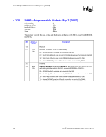
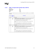
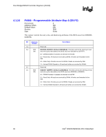
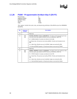
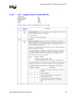
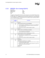
Host Bridge/DRAM Controller Registers (D0:F0) R 4.1.27 LAC-Legacy Access Control (D0:F0) PCI Device: Address Offset: Default Value: Access: Size: 0 97h 00h R/W 8 bits This 8-bit register controls a fixed DRAM hole from 15-16 MB. Bit Access & Default Description 7 R/W Hole Enable (HEN): This field enables a memory hole in DRAM space. The DRAM 0b that lies "behind" this space is not remapped. 0 = No memory hole. 1 = Memory hole from 15 MB to 16 MB. 6:1 Reserved 0 R/W MDA Present (MDAP): This bit works with the VGA Enable bits in the BCTRL 0b register of Device 1 to control the routing of processor initiated transactions targeting MDA compatible I/O and memory address ranges. This bit should not be set if device 1's VGA Enable bit is not set. If device 1's VGA enable bit is not set, then accesses to I/O address range x3BCh- x3BFh are forwarded to the DMI. If the VGA enable bit is set and MDA is not present, then accesses to I/O address range x3BCh-x3BFh are forwarded to PCI Express* if the address is within the corresponding IOBASE and IOLIMIT, otherwise they are forwarded to the DMI. MDA resources are defined as the following: Memory: 0B0000h - 0B7FFFh I/O: 3B4h, 3B5h, 3B8h, 3B9h, 3BAh, 3BFh, (Including ISA address aliases, A [15:10] are not used in decode) Any I/O reference that includes the I/O locations listed above, or their aliases, will be forwarded to the DMI even if the reference includes I/O locations not listed above. The following table shows the behavior for all combinations of MDA and VGA: VGAEN MDAP Description 0 0 All References to MDA and VGA space are routed to the DMI 0 1 Illegal combination 1 0 All VGA and MDA references are routed to PCI Express Graphics Attach. 1 1 All VGA references are routed to PCI Express Graphics Attach. MDA references are routed to the DMI Intel® 82925X/82925XE MCH Datasheet 69
-
 1
1 -
2
-
3
-
4
-
5
-
6
-
7
-
8
-
9
-
10
-
11
-
12
-
13
-
14
-
15
-
16
-
17
-
18
-
19
-
20
-
21
-
22
-
23
-
24
-
25
-
26
-
27
-
28
-
29
-
30
-
31
-
32
-
33
-
34
-
35
-
36
-
37
-
38
-
39
-
40
-
41
-
42
-
43
-
44
-
45
-
46
-
47
-
48
-
49
-
50
-
51
-
52
-
53
-
54
-
55
-
56
-
57
-
58
-
59
-
60
-
61
-
62
-
63
-
 64
64 -
 65
65 -
 66
66 -
 67
67 -
 68
68 -
 69
69 -
 70
70 -
 71
71 -
 72
72 -
 73
73 -
 74
74 -
75
-
76
-
77
-
78
-
79
-
80
-
81
-
82
-
83
-
84
-
85
-
86
-
87
-
88
-
89
-
90
-
91
-
92
-
93
-
94
-
95
-
96
-
97
-
98
-
99
-
100
-
101
-
102
-
103
-
104
-
105
-
106
-
107
-
108
-
109
-
110
-
111
-
112
-
113
-
114
-
115
-
116
-
117
-
118
-
119
-
120
-
121
-
122
-
123
-
124
-
125
-
126
-
127
-
128
-
129
-
130
-
131
-
132
-
133
-
134
-
135
-
136
-
137
-
138
-
139
-
140
-
141
-
142
-
143
-
144
-
145
-
146
-
147
-
148
-
149
-
150
-
151
-
152
-
153
-
154
-
155
-
156
-
157
-
158
-
159
-
160
-
161
-
162
-
163
-
164
-
165
-
166
-
167
-
168
-
169
-
170
-
171
-
172
-
173
-
174
-
175
-
176
-
177
-
178
-
179
-
180
-
181
-
182
-
183
-
184
-
185
-
186
-
187
-
188
-
189
-
190
-
191
-
192
-
193
-
194
-
195
-
196
-
197
-
198
-
199
-
200
-
201
-
202
-
203
-
204
-
205
-
206
-
207
-
208
-
209
-
210
-
211
-
212
-
213
-
214
-
215
-
216
-
217
-
218
-
219
-
220
-
221
-
222
-
223
-
224
-
225
-
226
-
227
-
228
-
229
-
230
-
231
-
232
-
233
-
234
-
235
-
236
-
237
-
238
-
239
-
240
-
241
-
242
 |
 |
