Intel 925 Data Sheet - Page 40
PCI Express* Enhanced Configuration Mechanism
 |
UPC - 683728067724
View all Intel 925 manuals
Add to My Manuals
Save this manual to your list of manuals |
Page 40 highlights
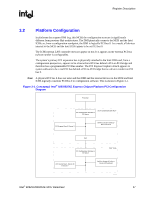
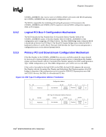
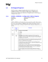
Register Description R Figure 3-3. DMI Type 1 Configuration Address Translation 31 30 1 Reserved Configuration Address 24 23 Bus Number 16 15 11 10 87 21 0 Device Number Function Double Word XX 3.3.4 31 30 1 OCFBh Reserved DMI Type 1 Configuration Address Extension 24 23 OCFAh Bus Number OCF9h 16 15 11 10 OCF8h 87 21 0 Device Number Function Double Word 00 DMI_Typ1_Config PCI Express* Enhanced Configuration Mechanism PCI Express extends the configuration space to 4096 bytes per device/function as compared to 256 bytes allowed by PCI Specification, Revision 2.3. PCI Express configuration space is divided into a PCI 2.3 compatible region that consists of the first 256B of a logical device's configuration space and a PCI Express extended region that consists of the remaining configuration space. The PCI compatible region can be accessed using either the mechanism defined in the previous section or using the enhanced PCI Express configuration access mechanism described in this section. The extended configuration registers may only be accessed using the enhanced PCI Express configuration access mechanism. To maintain compatibility with PCI configuration addressing mechanisms, system software must access the extended configuration space using 32bit operations (32-bit aligned) only. These 32-bit operations include byte enables allowing only appropriate bytes within the DWord to be accessed. Locked transactions to the PCI Express memory mapped configuration address space are not supported. All changes made using either access mechanism are equivalent. The enhanced PCI Express configuration access mechanism uses a flat memory-mapped address space to access device configuration registers. This address space is reported by the system firmware to the operating system. The PCIEXBAR register defines the base address for the 256-MB block of addresses below top of addressable memory (currently 4 GB) for the configuration space associated with all devices and functions that are potentially a part of the PCI Express root complex hierarchy. The PCI Express Configuration Transaction Header includes an additional 4 bits (Extended Register Address[3:0]) between the Function Number and Register Address fields to provide indexing into the 4 KB of configuration space allocated to each potential device. For PCI Compatible Configuration Requests, the Extended Register Address field must be all zeros. 40 Intel® 82925X/82925XE MCH Datasheet
-
 1
1 -
2
-
3
-
4
-
5
-
6
-
7
-
8
-
9
-
10
-
11
-
12
-
13
-
14
-
15
-
16
-
17
-
18
-
19
-
20
-
21
-
22
-
23
-
24
-
25
-
26
-
27
-
28
-
29
-
30
-
31
-
32
-
33
-
34
-
 35
35 -
 36
36 -
 37
37 -
 38
38 -
 39
39 -
 40
40 -
 41
41 -
 42
42 -
 43
43 -
 44
44 -
 45
45 -
46
-
47
-
48
-
49
-
50
-
51
-
52
-
53
-
54
-
55
-
56
-
57
-
58
-
59
-
60
-
61
-
62
-
63
-
64
-
65
-
66
-
67
-
68
-
69
-
70
-
71
-
72
-
73
-
74
-
75
-
76
-
77
-
78
-
79
-
80
-
81
-
82
-
83
-
84
-
85
-
86
-
87
-
88
-
89
-
90
-
91
-
92
-
93
-
94
-
95
-
96
-
97
-
98
-
99
-
100
-
101
-
102
-
103
-
104
-
105
-
106
-
107
-
108
-
109
-
110
-
111
-
112
-
113
-
114
-
115
-
116
-
117
-
118
-
119
-
120
-
121
-
122
-
123
-
124
-
125
-
126
-
127
-
128
-
129
-
130
-
131
-
132
-
133
-
134
-
135
-
136
-
137
-
138
-
139
-
140
-
141
-
142
-
143
-
144
-
145
-
146
-
147
-
148
-
149
-
150
-
151
-
152
-
153
-
154
-
155
-
156
-
157
-
158
-
159
-
160
-
161
-
162
-
163
-
164
-
165
-
166
-
167
-
168
-
169
-
170
-
171
-
172
-
173
-
174
-
175
-
176
-
177
-
178
-
179
-
180
-
181
-
182
-
183
-
184
-
185
-
186
-
187
-
188
-
189
-
190
-
191
-
192
-
193
-
194
-
195
-
196
-
197
-
198
-
199
-
200
-
201
-
202
-
203
-
204
-
205
-
206
-
207
-
208
-
209
-
210
-
211
-
212
-
213
-
214
-
215
-
216
-
217
-
218
-
219
-
220
-
221
-
222
-
223
-
224
-
225
-
226
-
227
-
228
-
229
-
230
-
231
-
232
-
233
-
234
-
235
-
236
-
237
-
238
-
239
-
240
-
241
-
242
 |
 |
