Intel 925 Data Sheet - Page 187
Signal Groups, PCI Express, Analog, HVCMOS, SSTL-1.8
 |
UPC - 683728067724
View all Intel 925 manuals
Add to My Manuals
Save this manual to your list of manuals |
Page 187 highlights
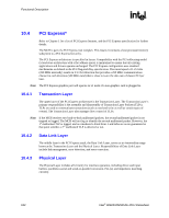
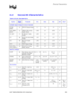
Electrical Characteristics R 11.3 Signal Groups The signal description includes the type of buffer used for the particular signal: GTL+ Open Drain GTL+ interface signal. Refer to the GTL+ I/O Specification for complete details. The MCH integrates most GTL+ termination resistors. DDR2 DDR2 System Memory (1.8 V CMOS buffers)(1.9 V CMOS buffers for DDR 533 CAS timing 3-3-3) PCI Express* PCI Express Interface Signals. These signals are compatible with the PCI Express Interface Specification 1.0a signaling environment AC specifications. The buffers are not 3.3V tolerant. Analog Analog signal interface. Ref Voltage reference signal. HVCMOS 2.5 V tolerant high voltage CMOS buffers. SSTL-1.8 1.8 V tolerant stub series termination logic. Table 11-4. Signal Groups Signal Group Signal Type Signals Notes Host Interface Signal Groups (a) GTL+ Input/Outputs HADS#, HBNR#, HBREQ0#, HDBSY#, HDRDY#, HDINV[3:0]#, HA[31:3]#, HADSTB[1:0]#, HD[63:0], HDSTBP[3:0]#, HDSTBN[3:0]#, HHIT#, HHITM#, HREQ[4:0]#, HLOCK# (b) GTL+ HBPRI#, HCPURST#, HDEFER#, HTRDY#, HRS[2:0]#, Common Clock Outputs HDPWR#, HEDRDY# (c) GTL+ Asynchronous Input BSEL[2:0], HPCREQ# (d) Analog Host I/F Ref & HVREF, HSWING HRCOMP, HSCOMP Comp. Signals PCI Express* Interface Signal Groups (e) PCI Express* Input PCI Express Interface: EXP_RXN(15:0), EXP_RXP(15:0), (f) PCI Express Output PCI Express Interface: EXP_TXN(15:0), EXP_TXP(15:0) (g) Analog EXP_COMP0 PCI Express I/F EXP_COMPI Compensation Signals Intel® 82925X/82925XE MCH Datasheet 187
-
 1
1 -
2
-
3
-
4
-
5
-
6
-
7
-
8
-
9
-
10
-
11
-
12
-
13
-
14
-
15
-
16
-
17
-
18
-
19
-
20
-
21
-
22
-
23
-
24
-
25
-
26
-
27
-
28
-
29
-
30
-
31
-
32
-
33
-
34
-
35
-
36
-
37
-
38
-
39
-
40
-
41
-
42
-
43
-
44
-
45
-
46
-
47
-
48
-
49
-
50
-
51
-
52
-
53
-
54
-
55
-
56
-
57
-
58
-
59
-
60
-
61
-
62
-
63
-
64
-
65
-
66
-
67
-
68
-
69
-
70
-
71
-
72
-
73
-
74
-
75
-
76
-
77
-
78
-
79
-
80
-
81
-
82
-
83
-
84
-
85
-
86
-
87
-
88
-
89
-
90
-
91
-
92
-
93
-
94
-
95
-
96
-
97
-
98
-
99
-
100
-
101
-
102
-
103
-
104
-
105
-
106
-
107
-
108
-
109
-
110
-
111
-
112
-
113
-
114
-
115
-
116
-
117
-
118
-
119
-
120
-
121
-
122
-
123
-
124
-
125
-
126
-
127
-
128
-
129
-
130
-
131
-
132
-
133
-
134
-
135
-
136
-
137
-
138
-
139
-
140
-
141
-
142
-
143
-
144
-
145
-
146
-
147
-
148
-
149
-
150
-
151
-
152
-
153
-
154
-
155
-
156
-
157
-
158
-
159
-
160
-
161
-
162
-
163
-
164
-
165
-
166
-
167
-
168
-
169
-
170
-
171
-
172
-
173
-
174
-
175
-
176
-
177
-
178
-
179
-
180
-
181
-
 182
182 -
 183
183 -
 184
184 -
 185
185 -
 186
186 -
 187
187 -
 188
188 -
 189
189 -
 190
190 -
 191
191 -
 192
192 -
193
-
194
-
195
-
196
-
197
-
198
-
199
-
200
-
201
-
202
-
203
-
204
-
205
-
206
-
207
-
208
-
209
-
210
-
211
-
212
-
213
-
214
-
215
-
216
-
217
-
218
-
219
-
220
-
221
-
222
-
223
-
224
-
225
-
226
-
227
-
228
-
229
-
230
-
231
-
232
-
233
-
234
-
235
-
236
-
237
-
238
-
239
-
240
-
241
-
242
 |
 |