Intel 925 Data Sheet - Page 76
SCICMD-SCI Command D0:F0, SKPD-Scratchpad Data D0:F0
 |
UPC - 683728067724
View all Intel 925 manuals
Add to My Manuals
Save this manual to your list of manuals |
Page 76 highlights
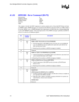
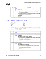
Host Bridge/DRAM Controller Registers (D0:F0) R 4.1.34 4.1.35 SCICMD-SCI Command (D0:F0) PCI Device: Address Offset: Default Value: Access: Size: 0 CEh 0000h R/W 16 bits This register enables various errors to generate an SMI DMI special cycle. When an error flag is set in the ERRSTS register, it can generate an SERR, SMI, or SCI DMI special cycle when enabled in the ERRCMD, SMICMD, or SCICMD registers, respectively. Note that one and only one message type can be enabled. Bit Access & Default Description 15:2 Reserved 1 R/W 0b 82925X MCH SCI on Multiple-Bit DRAM ECC Error (DMESCI): 1 = The MCH generates an SCI DMI message when it detects a multiple-bit error reported by the DRAM controller. 0 = Reporting of this condition via SCI messaging is disabled. For systems not supporting ECC this bit must be disabled. 82925XE MCH Reserved 0 R/W 0b 82925X MCH SCI on Single-bit ECC Error (DSESCI): 1 = The MCH generates an SCI DMI special cycle when the DRAM controller detects a single bit error. 0 = Reporting of this condition via SCI messaging is disabled. For systems that do not support ECC this bit must be disabled. 82925XE MCH Reserved SKPD-Scratchpad Data (D0:F0) PCI Device: Address Offset: Default Value: Access: Size: 0 DCh 00000000h R/W 32 bits This register holds 32 writable bits with no functionality behind them. It is for the convenience of BIOS and graphics drivers. Bit Access & Default Description 31:0 R/W Scratchpad Data: 1 DWord of data storage. 00000000 h 76 Intel® 82925X/82925XE MCH Datasheet
-
 1
1 -
2
-
3
-
4
-
5
-
6
-
7
-
8
-
9
-
10
-
11
-
12
-
13
-
14
-
15
-
16
-
17
-
18
-
19
-
20
-
21
-
22
-
23
-
24
-
25
-
26
-
27
-
28
-
29
-
30
-
31
-
32
-
33
-
34
-
35
-
36
-
37
-
38
-
39
-
40
-
41
-
42
-
43
-
44
-
45
-
46
-
47
-
48
-
49
-
50
-
51
-
52
-
53
-
54
-
55
-
56
-
57
-
58
-
59
-
60
-
61
-
62
-
63
-
64
-
65
-
66
-
67
-
68
-
69
-
70
-
 71
71 -
 72
72 -
 73
73 -
 74
74 -
 75
75 -
 76
76 -
 77
77 -
 78
78 -
 79
79 -
 80
80 -
 81
81 -
82
-
83
-
84
-
85
-
86
-
87
-
88
-
89
-
90
-
91
-
92
-
93
-
94
-
95
-
96
-
97
-
98
-
99
-
100
-
101
-
102
-
103
-
104
-
105
-
106
-
107
-
108
-
109
-
110
-
111
-
112
-
113
-
114
-
115
-
116
-
117
-
118
-
119
-
120
-
121
-
122
-
123
-
124
-
125
-
126
-
127
-
128
-
129
-
130
-
131
-
132
-
133
-
134
-
135
-
136
-
137
-
138
-
139
-
140
-
141
-
142
-
143
-
144
-
145
-
146
-
147
-
148
-
149
-
150
-
151
-
152
-
153
-
154
-
155
-
156
-
157
-
158
-
159
-
160
-
161
-
162
-
163
-
164
-
165
-
166
-
167
-
168
-
169
-
170
-
171
-
172
-
173
-
174
-
175
-
176
-
177
-
178
-
179
-
180
-
181
-
182
-
183
-
184
-
185
-
186
-
187
-
188
-
189
-
190
-
191
-
192
-
193
-
194
-
195
-
196
-
197
-
198
-
199
-
200
-
201
-
202
-
203
-
204
-
205
-
206
-
207
-
208
-
209
-
210
-
211
-
212
-
213
-
214
-
215
-
216
-
217
-
218
-
219
-
220
-
221
-
222
-
223
-
224
-
225
-
226
-
227
-
228
-
229
-
230
-
231
-
232
-
233
-
234
-
235
-
236
-
237
-
238
-
239
-
240
-
241
-
242
 |
 |