Intel 925 Data Sheet - Page 170

SMM Access through GTT TLB, Memory Shadowing, I/O Address Space

Page 170 highlights

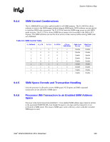
System Address Map R 9.4.7 9.4.8 9.4.9 SMM Access through GTT TLB Accesses through GTT TLB address translation to enabled SMM DRAM space are not allowed. Writes will be routed to memory address 0h with byte enables de-asserted and reads will be routed to memory address 0h. If a GTT TLB translated address hits enabled SMM DRAM space, an Invalid Translation Table Entry Flag is reported to BIOS. PCI Express and DMI originated accesses are never allowed to access SMM space directly or through the GTT TLB address translation. If a GTT TLB translated address hits enabled SMM DRAM space, an Invalid Translation Table Entry Flag is reported to BIOS. PCI Express and DMI write accesses through the graphics memory range set up by BIOS will be snooped. If, when translated, the resulting physical address is to enabled SMM DRAM space, the request will be remapped to address 0h with de-asserted byte enables. PCI Express and DMI read accesses to the graphics memory range set up by BIOS are not supported; therefore, users/systems will be remapped to address 0h. The read will complete with UR (unsupported request) completion status. GTT fetches are always decoded (at fetch time) to ensure they are not in SMM (actually, anything above base of TSEG or 640 KB-1 MB). Thus, they will be invalid and go to address 0h. This is not specific to PCI Express or DMI; it applies to the processor. Also, since the graphics memory range snoop would not be directly to SMM space, there would not be a writeback to SMM. In fact, the writeback would also be invalid (because it uses the same translation) and goes to address 0h. Memory Shadowing Any block of memory that can be designated as "read only" or "write only" can be "shadowed" into MCH main memory. Typically, this is done to allow ROM code to execute more rapidly out of main DRAM memory. ROM is used as read-only during the copy process while main DRAM memory at the same time is designated write-only. After copying, the main DRAM memory is designated read-only so that ROM is shadowed. Processor bus transactions are routed accordingly. I/O Address Space The MCH does not support the existence of any other I/O devices beside itself on the processor bus. The MCH generates either DMI or PCI Express bus cycles for all processor I/O accesses that it does not claim. Within the host bridge, the MCH contains two internal registers in the processor I/O space. These locations are used to implement a configuration space access mechanism. The processor allows 64 KB+3 bytes to be addressed within the I/O space. The MCH propagates the processor I/O address without any translation on to the destination bus; therefore, providing addressability for 64 KB+3 byte locations. Note that the upper 3 locations can be accessed only during I/O address wrap-around when processor bus HA16# address signal is asserted. HA16# is asserted on the processor bus when an I/O access is made to 4 bytes from address 0FFFDh, 0FFFEh, or 0FFFFh. HA16# is also asserted when an I/O access is made to 2 bytes from address 0FFFFh. 170 Intel® 82925X/82925XE MCH Datasheet

  • 1
  • 2
  • 3
  • 4
  • 5
  • 6
  • 7
  • 8
  • 9
  • 10
  • 11
  • 12
  • 13
  • 14
  • 15
  • 16
  • 17
  • 18
  • 19
  • 20
  • 21
  • 22
  • 23
  • 24
  • 25
  • 26
  • 27
  • 28
  • 29
  • 30
  • 31
  • 32
  • 33
  • 34
  • 35
  • 36
  • 37
  • 38
  • 39
  • 40
  • 41
  • 42
  • 43
  • 44
  • 45
  • 46
  • 47
  • 48
  • 49
  • 50
  • 51
  • 52
  • 53
  • 54
  • 55
  • 56
  • 57
  • 58
  • 59
  • 60
  • 61
  • 62
  • 63
  • 64
  • 65
  • 66
  • 67
  • 68
  • 69
  • 70
  • 71
  • 72
  • 73
  • 74
  • 75
  • 76
  • 77
  • 78
  • 79
  • 80
  • 81
  • 82
  • 83
  • 84
  • 85
  • 86
  • 87
  • 88
  • 89
  • 90
  • 91
  • 92
  • 93
  • 94
  • 95
  • 96
  • 97
  • 98
  • 99
  • 100
  • 101
  • 102
  • 103
  • 104
  • 105
  • 106
  • 107
  • 108
  • 109
  • 110
  • 111
  • 112
  • 113
  • 114
  • 115
  • 116
  • 117
  • 118
  • 119
  • 120
  • 121
  • 122
  • 123
  • 124
  • 125
  • 126
  • 127
  • 128
  • 129
  • 130
  • 131
  • 132
  • 133
  • 134
  • 135
  • 136
  • 137
  • 138
  • 139
  • 140
  • 141
  • 142
  • 143
  • 144
  • 145
  • 146
  • 147
  • 148
  • 149
  • 150
  • 151
  • 152
  • 153
  • 154
  • 155
  • 156
  • 157
  • 158
  • 159
  • 160
  • 161
  • 162
  • 163
  • 164
  • 165
  • 166
  • 167
  • 168
  • 169
  • 170
  • 171
  • 172
  • 173
  • 174
  • 175
  • 176
  • 177
  • 178
  • 179
  • 180
  • 181
  • 182
  • 183
  • 184
  • 185
  • 186
  • 187
  • 188
  • 189
  • 190
  • 191
  • 192
  • 193
  • 194
  • 195
  • 196
  • 197
  • 198
  • 199
  • 200
  • 201
  • 202
  • 203
  • 204
  • 205
  • 206
  • 207
  • 208
  • 209
  • 210
  • 211
  • 212
  • 213
  • 214
  • 215
  • 216
  • 217
  • 218
  • 219
  • 220
  • 221
  • 222
  • 223
  • 224
  • 225
  • 226
  • 227
  • 228
  • 229
  • 230
  • 231
  • 232
  • 233
  • 234
  • 235
  • 236
  • 237
  • 238
  • 239
  • 240
  • 241
  • 242

System Address Map
R
170
Intel
®
82925X/82925XE MCH Datasheet
9.4.7
SMM Access through GTT TLB
Accesses through GTT TLB address translation to enabled SMM DRAM space are not allowed.
Writes will be routed to memory address 0h with byte enables de-asserted and reads will be
routed to memory address 0h. If a GTT TLB translated address hits enabled SMM DRAM space,
an Invalid Translation Table Entry Flag is reported to BIOS.
PCI Express and DMI originated accesses are
never
allowed to access SMM space directly or
through the GTT TLB address translation. If a GTT TLB translated address hits enabled SMM
DRAM space, an Invalid Translation Table Entry Flag is reported to BIOS.
PCI Express and DMI write accesses through the graphics memory range set up by BIOS will be
snooped. If, when translated, the resulting physical address is to enabled SMM DRAM space, the
request will be remapped to address 0h with de-asserted byte enables.
PCI Express and DMI read accesses to the graphics memory range set up by BIOS are not
supported; therefore, users/systems will be remapped to address 0h. The read will complete with
UR (unsupported request) completion status.
GTT fetches are always decoded (at fetch time) to ensure they are not in SMM (actually, anything
above base of TSEG or 640 KB–1 MB). Thus, they will be invalid and go to address 0h. This is
not specific to PCI Express or DMI; it applies to the processor. Also, since the graphics memory
range snoop would not be directly to SMM space, there would not be a writeback to SMM. In
fact, the writeback would also be invalid (because it uses the same translation) and goes to
address 0h.
9.4.8
Memory Shadowing
Any block of memory that can be designated as “read only” or “write only” can be “shadowed”
into MCH main memory. Typically, this is done to allow ROM code to execute more rapidly out
of main DRAM memory. ROM is used as read-only during the copy process while main DRAM
memory at the same time is designated write-only. After copying, the main DRAM memory is
designated read-only so that ROM is shadowed. Processor bus transactions are routed
accordingly.
9.4.9
I/O Address Space
The MCH does not support the existence of any other I/O devices beside itself on the processor
bus. The MCH generates either DMI or PCI Express bus cycles for all processor I/O accesses that
it does not claim. Within the host bridge, the MCH contains two internal registers in the processor
I/O space. These locations are used to implement a configuration space access mechanism.
The processor allows 64 KB+3 bytes to be addressed within the I/O space. The MCH propagates
the processor I/O address without any translation on to the destination bus; therefore, providing
addressability for 64 KB+3 byte locations. Note that the upper 3 locations can be accessed only
during I/O address wrap-around when processor bus HA16# address signal is asserted. HA16# is
asserted on the processor bus when an I/O access is made to 4 bytes from address 0FFFDh,
0FFFEh, or 0FFFFh. HA16# is also asserted when an I/O access is made to
2 bytes from address 0FFFFh.