Intel 925 Data Sheet - Page 56
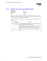
PCIEXBAR-PCI Express* Register Range Base Address, D0:F0
 |
UPC - 683728067724
View all Intel 925 manuals
Add to My Manuals
Save this manual to your list of manuals |
Page 56 highlights
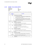
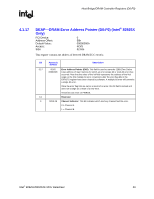
Host Bridge/DRAM Controller Registers (D0:F0) R 4.1.14 PCIEXBAR-PCI Express* Register Range Base Address (D0:F0) PCI Device: Address Offset: Default Value: Access: Size: 0 48h E0000000h R/W 32 bits This is the base address for the PCI Express configuration space. This window of addresses contains the 4 KB of configuration space for each PCI Express device that can potentially be part of the PCI Express hierarchy associated with the MCH. There is not actual physical memory within this 256-MB window that can be addressed. Each PCI Express hierarchies require a PCI Express BASE register. The MCH supports one PCI Express hierarchy. The 256 MB reserved by this register does not alias to any PCI 2.3 compliant memory-mapped space. For example, MCHBAR reserves a 16-KB space and reserves a 4-KB space both outside of PCIEXBAR space. They cannot be overlaid on the space reserved by PCIEXBAR for devices 0. On reset, this register is disabled and must be enabled by writing a 1 to PCIEXBAREN [Dev 0, offset 54h, bit 31] If the PCI Express Base Address [bits 31:28] were set to Fh, an overlap with the High BIOS area, APIC ranges would result. Software must guarantee that these ranges do not overlap. The PCI Express Base Address cannot be less than the maximum address written to the Top of physical memory register (TOLUD). If a system is populated with more than 3.5 GB, either the PCI Express Enhanced Access mechanism must be disabled or the value in TOLUD must be reduced to report that only 3.5 GB are present in the system to allow a value of Eh for the PCI Express Base Address (assuming that all PCI 2.3 compatible configuration space fits above 3.75 GB). Bit 31:28 27:0 Access & Default R/W Eh Description PCI Express* Base Address: This field corresponds to bits 31 to 28 of the base address for PCI Express enhanced configuration space. BIOS will program this register resulting in a base address for a 256-MB block of contiguous memory address space. Having control of those particular 4 bits insures that this base address will be on a 256-MB boundary, above the lowest 256 MB and still within total addressable memory space, currently 4 GB. The address used to access the PCI Express configuration space for a specific device can be determined as follows: PCI Express Base Address + Bus Number * 1 MB + Device Number * 32 KB + Function Number * 4 KB The address used to access the PCI Express configuration space for Device 1 in this component would be PCI Express Base Address + 0 * 1 MB + 1 * 32 KB + 0 * 4 KB = PCI Express Base Address + 32 KB. Remember that this address is the beginning of the 4-KB space that contains both the PCI compatible configuration space and the PCI Express extended configuration space. Reserved 56 Intel® 82925X/82925XE MCH Datasheet
-
 1
1 -
2
-
3
-
4
-
5
-
6
-
7
-
8
-
9
-
10
-
11
-
12
-
13
-
14
-
15
-
16
-
17
-
18
-
19
-
20
-
21
-
22
-
23
-
24
-
25
-
26
-
27
-
28
-
29
-
30
-
31
-
32
-
33
-
34
-
35
-
36
-
37
-
38
-
39
-
40
-
41
-
42
-
43
-
44
-
45
-
46
-
47
-
48
-
49
-
50
-
 51
51 -
 52
52 -
 53
53 -
 54
54 -
 55
55 -
 56
56 -
 57
57 -
 58
58 -
 59
59 -
 60
60 -
 61
61 -
62
-
63
-
64
-
65
-
66
-
67
-
68
-
69
-
70
-
71
-
72
-
73
-
74
-
75
-
76
-
77
-
78
-
79
-
80
-
81
-
82
-
83
-
84
-
85
-
86
-
87
-
88
-
89
-
90
-
91
-
92
-
93
-
94
-
95
-
96
-
97
-
98
-
99
-
100
-
101
-
102
-
103
-
104
-
105
-
106
-
107
-
108
-
109
-
110
-
111
-
112
-
113
-
114
-
115
-
116
-
117
-
118
-
119
-
120
-
121
-
122
-
123
-
124
-
125
-
126
-
127
-
128
-
129
-
130
-
131
-
132
-
133
-
134
-
135
-
136
-
137
-
138
-
139
-
140
-
141
-
142
-
143
-
144
-
145
-
146
-
147
-
148
-
149
-
150
-
151
-
152
-
153
-
154
-
155
-
156
-
157
-
158
-
159
-
160
-
161
-
162
-
163
-
164
-
165
-
166
-
167
-
168
-
169
-
170
-
171
-
172
-
173
-
174
-
175
-
176
-
177
-
178
-
179
-
180
-
181
-
182
-
183
-
184
-
185
-
186
-
187
-
188
-
189
-
190
-
191
-
192
-
193
-
194
-
195
-
196
-
197
-
198
-
199
-
200
-
201
-
202
-
203
-
204
-
205
-
206
-
207
-
208
-
209
-
210
-
211
-
212
-
213
-
214
-
215
-
216
-
217
-
218
-
219
-
220
-
221
-
222
-
223
-
224
-
225
-
226
-
227
-
228
-
229
-
230
-
231
-
232
-
233
-
234
-
235
-
236
-
237
-
238
-
239
-
240
-
241
-
242
 |
 |