Intel 925 Data Sheet - Page 86
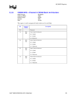
C0DRT1-Channel A DRAM Timing Register, MMIO Range, MCHBAR, Address Offset, Default Value, Access, R/W
 |
UPC - 683728067724
View all Intel 925 manuals
Add to My Manuals
Save this manual to your list of manuals |
Page 86 highlights
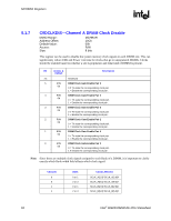
MCHBAR Registers R 5.1.9 C0DRT1-Channel A DRAM Timing Register MMIO Range: Address Offset: Default Value: Access: Size: MCHBAR 114h 900122hh R/W, RO 32 bits Bit 31:24 23:20 19 18:10 9:8 7 Access & Default R/W 9h RO 0b R/W 01b Description Reserved Activate to Precharge delay (tRAS). This bit controls the number of DRAM clocks for tRAS. Minimum recommendations are beside their corresponding encodings. 0h - 3h = Reserved 4h - Fh = Four to Fifteen Clocks respectively. Reserved for Activate to Precharge Delay (tRAS) MAX: It is required that the Panic Refresh timer be set to a value less than the tRAS maximum. Based on this setting, a Panic Refresh occurs before TRAS maximum expiration and closes all the banks. This bit controls the maximum number of clocks that a DRAM bank can remain open. After this time period, the DRAM controller will guarantee to pre-charge the bank. This time period may or may not be set to overlap with time period that requires a refresh to happen. The DRAM controller includes a separate tRAS-MAX counter for every supported bank. With a maximum of four ranks, and four banks per rank, there are 16 counters per channel. 0 = 120 microseconds 1 = Reserved Note: This register will become Read Only with a value of 0 if the design does not implement these counters. tRAS-MAX is not required because a panic refresh will close all banks in a rank before tRAS-MAX expires. Reserved CASB Latency (tCL). This value is programmable on DDR2 DIMMs. The value programmed here must match the CAS Latency of every DDR2 DIMM in the system. Encoding DDR2 CL 00 5 01 4 10 3 11 Reserved Reserved 86 Intel® 82925X/82925XE MCH Datasheet
-
 1
1 -
2
-
3
-
4
-
5
-
6
-
7
-
8
-
9
-
10
-
11
-
12
-
13
-
14
-
15
-
16
-
17
-
18
-
19
-
20
-
21
-
22
-
23
-
24
-
25
-
26
-
27
-
28
-
29
-
30
-
31
-
32
-
33
-
34
-
35
-
36
-
37
-
38
-
39
-
40
-
41
-
42
-
43
-
44
-
45
-
46
-
47
-
48
-
49
-
50
-
51
-
52
-
53
-
54
-
55
-
56
-
57
-
58
-
59
-
60
-
61
-
62
-
63
-
64
-
65
-
66
-
67
-
68
-
69
-
70
-
71
-
72
-
73
-
74
-
75
-
76
-
77
-
78
-
79
-
80
-
 81
81 -
 82
82 -
 83
83 -
 84
84 -
 85
85 -
 86
86 -
 87
87 -
 88
88 -
 89
89 -
 90
90 -
 91
91 -
92
-
93
-
94
-
95
-
96
-
97
-
98
-
99
-
100
-
101
-
102
-
103
-
104
-
105
-
106
-
107
-
108
-
109
-
110
-
111
-
112
-
113
-
114
-
115
-
116
-
117
-
118
-
119
-
120
-
121
-
122
-
123
-
124
-
125
-
126
-
127
-
128
-
129
-
130
-
131
-
132
-
133
-
134
-
135
-
136
-
137
-
138
-
139
-
140
-
141
-
142
-
143
-
144
-
145
-
146
-
147
-
148
-
149
-
150
-
151
-
152
-
153
-
154
-
155
-
156
-
157
-
158
-
159
-
160
-
161
-
162
-
163
-
164
-
165
-
166
-
167
-
168
-
169
-
170
-
171
-
172
-
173
-
174
-
175
-
176
-
177
-
178
-
179
-
180
-
181
-
182
-
183
-
184
-
185
-
186
-
187
-
188
-
189
-
190
-
191
-
192
-
193
-
194
-
195
-
196
-
197
-
198
-
199
-
200
-
201
-
202
-
203
-
204
-
205
-
206
-
207
-
208
-
209
-
210
-
211
-
212
-
213
-
214
-
215
-
216
-
217
-
218
-
219
-
220
-
221
-
222
-
223
-
224
-
225
-
226
-
227
-
228
-
229
-
230
-
231
-
232
-
233
-
234
-
235
-
236
-
237
-
238
-
239
-
240
-
241
-
242
 |
 |
