Intel 925 Data Sheet - Page 114
PCISTS1-PCI Status D1:F0
 |
UPC - 683728067724
View all Intel 925 manuals
Add to My Manuals
Save this manual to your list of manuals |
Page 114 highlights
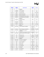
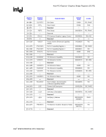
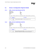
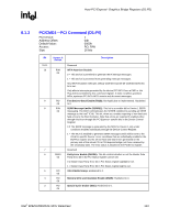
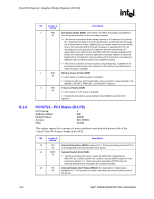
Host-PCI Express* Graphics Bridge Registers (D1:F0) R 8.1.4 Bit Access & Default Description 2 R/W Bus Master Enable (BME): This bit does not affect forwarding of completions 0b from the primary interface to the secondary interface. 0 = This device is prevented from making memory or I/O requests to its primary bus. Note that according to the PCI specification, as MSI interrupt messages are in-band memory writes, disabling the bus master enable bit prevents this device from generating MSI interrupt messages or passing them from its secondary bus to its primary bus. Upstream memory writes/reads, I/O writes/reads, peer writes/reads, and MSIs will all be treated as illegal cycles. Writes are forwarded to memory address 0h with byte enables de-asserted. Reads will be forwarded to memory address 0h and will return Unsupported Request status (or Master abort) in its completion packet. 1 = This device is allowed to issue requests to its primary bus. Completions for previously issued memory read requests on the primary bus will be issued when the data is available. 1 R/W Memory Access Enable (MAE) 0b 0 = All of device 1's memory space is disabled. 1 = Enable the Memory and Pre-fetchable memory address ranges defined in the MBASE1, MLIMIT1, PMBASE1, and PMLIMIT1 registers. 0 R/W IO Access Enable (IOAE) 0b 0 = All of device 1's I/O space is disabled. 1 = Enable the I/O address range defined in the IOBASE1 and IOLIMIT1 registers. PCISTS1-PCI Status (D1:F0) PCI Device: Address Offset: Default Value: Access: Size: 1 06h 0000h RO, R/W/C 16 bits This register reports the occurrence of error conditions associated with primary side of the "virtual" Host-PCI Express bridge in the MCH. Bit Access & Default Description 15 RO Detected Parity Error (DPE): Hardwired to 0. Parity (generating poisoned TLPs) 0b is not supported on the primary side of this device. 14 R/WC Signaled System Error (SSE): 0b 1 = This bit is set when this Device sends an SERR due to detecting an ERR_FATAL or ERR_NONFATAL condition and the SERR Enable bit in the Command register is '1'. Both received (if enabled by BCTRL1[1]) and internally detected error messages do not affect this field. 13 RO Received Master Abort Status (RMAS): Not Applicable or Implemented. 0b Hardwired to 0. The concept of a master abort does not exist on primary side of this device. 114 Intel® 82925X/82925XE MCH Datasheet
-
 1
1 -
2
-
3
-
4
-
5
-
6
-
7
-
8
-
9
-
10
-
11
-
12
-
13
-
14
-
15
-
16
-
17
-
18
-
19
-
20
-
21
-
22
-
23
-
24
-
25
-
26
-
27
-
28
-
29
-
30
-
31
-
32
-
33
-
34
-
35
-
36
-
37
-
38
-
39
-
40
-
41
-
42
-
43
-
44
-
45
-
46
-
47
-
48
-
49
-
50
-
51
-
52
-
53
-
54
-
55
-
56
-
57
-
58
-
59
-
60
-
61
-
62
-
63
-
64
-
65
-
66
-
67
-
68
-
69
-
70
-
71
-
72
-
73
-
74
-
75
-
76
-
77
-
78
-
79
-
80
-
81
-
82
-
83
-
84
-
85
-
86
-
87
-
88
-
89
-
90
-
91
-
92
-
93
-
94
-
95
-
96
-
97
-
98
-
99
-
100
-
101
-
102
-
103
-
104
-
105
-
106
-
107
-
108
-
 109
109 -
 110
110 -
 111
111 -
 112
112 -
 113
113 -
 114
114 -
 115
115 -
 116
116 -
 117
117 -
 118
118 -
 119
119 -
120
-
121
-
122
-
123
-
124
-
125
-
126
-
127
-
128
-
129
-
130
-
131
-
132
-
133
-
134
-
135
-
136
-
137
-
138
-
139
-
140
-
141
-
142
-
143
-
144
-
145
-
146
-
147
-
148
-
149
-
150
-
151
-
152
-
153
-
154
-
155
-
156
-
157
-
158
-
159
-
160
-
161
-
162
-
163
-
164
-
165
-
166
-
167
-
168
-
169
-
170
-
171
-
172
-
173
-
174
-
175
-
176
-
177
-
178
-
179
-
180
-
181
-
182
-
183
-
184
-
185
-
186
-
187
-
188
-
189
-
190
-
191
-
192
-
193
-
194
-
195
-
196
-
197
-
198
-
199
-
200
-
201
-
202
-
203
-
204
-
205
-
206
-
207
-
208
-
209
-
210
-
211
-
212
-
213
-
214
-
215
-
216
-
217
-
218
-
219
-
220
-
221
-
222
-
223
-
224
-
225
-
226
-
227
-
228
-
229
-
230
-
231
-
232
-
233
-
234
-
235
-
236
-
237
-
238
-
239
-
240
-
241
-
242
 |
 |
