Intel 925 Data Sheet - Page 169
SMM Control Combinations, SMM Space Decode and Transaction Handling
 |
UPC - 683728067724
View all Intel 925 manuals
Add to My Manuals
Save this manual to your list of manuals |
Page 169 highlights
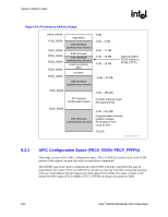
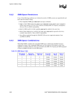
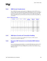
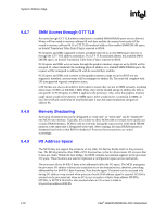
System Address Map R 9.4.4 SMM Control Combinations The G_SMRAME bit provides a global enable for all SMM memory. The D_OPEN bit allows software to write to the SMM ranges without being in SMM mode. BIOS software can use this bit to initialize SMM code at powerup. The D_LCK bit limits the SMM range access to only SMM mode accesses. The D_CLS bit causes SMM data accesses to be forwarded to the DMI or PCI Express. The SMM software can use this bit to write to video memory while running SMM code out of DRAM. Table 9-6. SMM Control Table G_SMRAME D_LCK 0 x 1 0 1 0 1 0 1 0 1 0 1 1 1 1 1 1 D_CLS X X 0 0 1 1 X 0 1 D_OPEN x 0 0 1 0 1 x x x CPU in SMM Mode x 0 1 x 1 x 0 1 1 SMM Code Access Disable Disable Enable Enable Enable Invalid Disable Enable Enable SMM Data Access Disable Disable Enable Enable Disable Invalid Disable Enable Disable 9.4.5 9.4.6 SMM Space Decode and Transaction Handling Only the processor is allowed to access SMM space. PCI Express and DMI originated transactions are not allowed to SMM space. Processor WB Transaction to an Enabled SMM Address Space Processor write-back transactions (HREQ1# = 0) to enabled SMM address space must be written to the associated SMM DRAM, even though the space is not open and the transaction is not performed in SMM mode. This ensures SMM space cache coherency when cacheable extended SMM space is used. Intel® 82925X/82925XE MCH Datasheet 169
-
 1
1 -
2
-
3
-
4
-
5
-
6
-
7
-
8
-
9
-
10
-
11
-
12
-
13
-
14
-
15
-
16
-
17
-
18
-
19
-
20
-
21
-
22
-
23
-
24
-
25
-
26
-
27
-
28
-
29
-
30
-
31
-
32
-
33
-
34
-
35
-
36
-
37
-
38
-
39
-
40
-
41
-
42
-
43
-
44
-
45
-
46
-
47
-
48
-
49
-
50
-
51
-
52
-
53
-
54
-
55
-
56
-
57
-
58
-
59
-
60
-
61
-
62
-
63
-
64
-
65
-
66
-
67
-
68
-
69
-
70
-
71
-
72
-
73
-
74
-
75
-
76
-
77
-
78
-
79
-
80
-
81
-
82
-
83
-
84
-
85
-
86
-
87
-
88
-
89
-
90
-
91
-
92
-
93
-
94
-
95
-
96
-
97
-
98
-
99
-
100
-
101
-
102
-
103
-
104
-
105
-
106
-
107
-
108
-
109
-
110
-
111
-
112
-
113
-
114
-
115
-
116
-
117
-
118
-
119
-
120
-
121
-
122
-
123
-
124
-
125
-
126
-
127
-
128
-
129
-
130
-
131
-
132
-
133
-
134
-
135
-
136
-
137
-
138
-
139
-
140
-
141
-
142
-
143
-
144
-
145
-
146
-
147
-
148
-
149
-
150
-
151
-
152
-
153
-
154
-
155
-
156
-
157
-
158
-
159
-
160
-
161
-
162
-
163
-
 164
164 -
 165
165 -
 166
166 -
 167
167 -
 168
168 -
 169
169 -
 170
170 -
 171
171 -
 172
172 -
 173
173 -
 174
174 -
175
-
176
-
177
-
178
-
179
-
180
-
181
-
182
-
183
-
184
-
185
-
186
-
187
-
188
-
189
-
190
-
191
-
192
-
193
-
194
-
195
-
196
-
197
-
198
-
199
-
200
-
201
-
202
-
203
-
204
-
205
-
206
-
207
-
208
-
209
-
210
-
211
-
212
-
213
-
214
-
215
-
216
-
217
-
218
-
219
-
220
-
221
-
222
-
223
-
224
-
225
-
226
-
227
-
228
-
229
-
230
-
231
-
232
-
233
-
234
-
235
-
236
-
237
-
238
-
239
-
240
-
241
-
242
 |
 |