Intel 925 Data Sheet - Page 176
System Memory Configuration Register Overview, DRAM Rank Boundary CxDRBy
 |
UPC - 683728067724
View all Intel 925 manuals
Add to My Manuals
Save this manual to your list of manuals |
Page 176 highlights
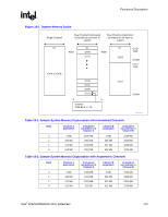
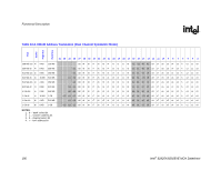
Functional Description R 10.3 System Memory Configuration Register Overview The configuration registers located in the PCI configuration space of the MCH control the system memory operation. Following is a brief description of configuration registers. • DRAM Rank Boundary (CxDRBy): The x represents a channel, either A (where x = 0) or B (where x = 1). The y represents a rank, 0 through 3. DRB registers define the upper addresses for a rank of DRAM devices in a channel. When the MCH is configured in asymmetric mode, each register represents a single rank. When the MCH is configured in a dual interleaved mode, each register represents a pair of corresponding ranks in opposing channels. There are 4 DRB registers for each channel. • DRAM Rank Architecture (CxDRAy): The x represents a channel, either A (where x = 0) or B (where x = 1). The y represents a rank, 0 through 3. DRA registers specify the architecture features of each rank of devices in a channel. The only architecture feature specified is page size. When the MCH is configured in asymmetric mode, each DRA represents a single rank in a single channel. When the MCH is configured in a dual-channel lock-step or interleaved mode, each DRA represents a pair of corresponding ranks in opposing channels. There are 4 DRA registers per channel. Each requires only 3 bits, so there are two DRAs packed into a byte. • Clock Configuration (CLKCFG): Specifies DRAM frequency. The same clock frequency will be driven to all DIMMs. • DRAM Timing (CxDRTy): The x represents a channel, A (where x = 0) or B (where x = 1). A second register for a channel is differentiated by y, A or B. The DRT registers define the timing parameters for all devices in a channel. The BIOS programs this register with "least common denominator" values after reading the SPD registers of each DIMM in the channel. • DRAM Control (CxDRCy): The x represents a channel, A (where x = 0) or B (where x = 1). A second register for a channel is differentiated by y, A or B. DRAM refresh mode, rate, and other controls are selected here. 176 Intel® 82925X/82925XE MCH Datasheet
-
 1
1 -
2
-
3
-
4
-
5
-
6
-
7
-
8
-
9
-
10
-
11
-
12
-
13
-
14
-
15
-
16
-
17
-
18
-
19
-
20
-
21
-
22
-
23
-
24
-
25
-
26
-
27
-
28
-
29
-
30
-
31
-
32
-
33
-
34
-
35
-
36
-
37
-
38
-
39
-
40
-
41
-
42
-
43
-
44
-
45
-
46
-
47
-
48
-
49
-
50
-
51
-
52
-
53
-
54
-
55
-
56
-
57
-
58
-
59
-
60
-
61
-
62
-
63
-
64
-
65
-
66
-
67
-
68
-
69
-
70
-
71
-
72
-
73
-
74
-
75
-
76
-
77
-
78
-
79
-
80
-
81
-
82
-
83
-
84
-
85
-
86
-
87
-
88
-
89
-
90
-
91
-
92
-
93
-
94
-
95
-
96
-
97
-
98
-
99
-
100
-
101
-
102
-
103
-
104
-
105
-
106
-
107
-
108
-
109
-
110
-
111
-
112
-
113
-
114
-
115
-
116
-
117
-
118
-
119
-
120
-
121
-
122
-
123
-
124
-
125
-
126
-
127
-
128
-
129
-
130
-
131
-
132
-
133
-
134
-
135
-
136
-
137
-
138
-
139
-
140
-
141
-
142
-
143
-
144
-
145
-
146
-
147
-
148
-
149
-
150
-
151
-
152
-
153
-
154
-
155
-
156
-
157
-
158
-
159
-
160
-
161
-
162
-
163
-
164
-
165
-
166
-
167
-
168
-
169
-
170
-
 171
171 -
 172
172 -
 173
173 -
 174
174 -
 175
175 -
 176
176 -
 177
177 -
 178
178 -
 179
179 -
 180
180 -
 181
181 -
182
-
183
-
184
-
185
-
186
-
187
-
188
-
189
-
190
-
191
-
192
-
193
-
194
-
195
-
196
-
197
-
198
-
199
-
200
-
201
-
202
-
203
-
204
-
205
-
206
-
207
-
208
-
209
-
210
-
211
-
212
-
213
-
214
-
215
-
216
-
217
-
218
-
219
-
220
-
221
-
222
-
223
-
224
-
225
-
226
-
227
-
228
-
229
-
230
-
231
-
232
-
233
-
234
-
235
-
236
-
237
-
238
-
239
-
240
-
241
-
242
 |
 |