Intel 925 Data Sheet - Page 136
DCTL-Device Control D1:F0, ERR_NONFATAL
 |
UPC - 683728067724
View all Intel 925 manuals
Add to My Manuals
Save this manual to your list of manuals |
Page 136 highlights
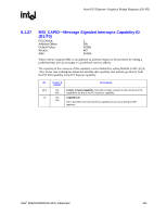
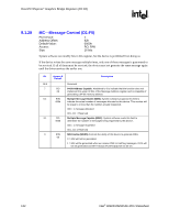
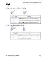
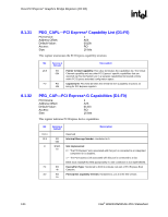
Host-PCI Express* Graphics Bridge Registers (D1:F0) R 8.1.34 DCTL-Device Control (D1:F0) PCI Device: Address Offset: Default Value: Access: Size: 1 A8h 0000h R/W 16 bits This register provides control for PCI Express device specific capabilities. The error reporting enable bits are in reference to errors detected by this device, not error messages received across the link. The reporting of error messages (ERR_CORR, ERR_NONFATAL, ERR_FATAL) received by Root Port is controlled exclusively by Root Port Command Register. Bit Access & Default Description 15:8 Reserved 7:5 R/W Max Payload Size 000b 000 = 128B maximum supported payload for Transaction Layer Packets (TLP). As a receiver, the device must handle TLPs as large as the set value; as transmitter, the device must not generate TLPs exceeding the set value. Note: All other encodings are reserved. 4 Reserved 3 R/W Unsupported Request Reporting Enable: 0b 0 = Disable. 1 = Enable. Unsupported Requests will be reported. Note that reporting of error messages received by Root Port is controlled exclusively by Root Control register. 2 R/W Fatal Error Reporting Enable: 0b 0 = Disable. 1 = Enable. Fatal errors will be reported. For a Root Port, the reporting of fatal errors is internal to the root. No external ERR_FATAL message is generated. 1 R/W Non-Fatal Error Reporting Enable: 0b 0 = Disable. 1 = Enable. Non-fatal errors will be reported. For a Root Port, the reporting of non-fatal errors is internal to the root. No external ERR_NONFATAL message is generated. Uncorrectable errors can result in degraded performance. 0 R/W Correctable Error Reporting Enable: 0b 0 = Disable. 1 = Enable. Correctable errors will be reported. For a Root Port, the reporting of correctable errors is internal to the root. No external ERR_CORR message is generated. 136 Intel® 82925X/82925XE MCH Datasheet
-
 1
1 -
2
-
3
-
4
-
5
-
6
-
7
-
8
-
9
-
10
-
11
-
12
-
13
-
14
-
15
-
16
-
17
-
18
-
19
-
20
-
21
-
22
-
23
-
24
-
25
-
26
-
27
-
28
-
29
-
30
-
31
-
32
-
33
-
34
-
35
-
36
-
37
-
38
-
39
-
40
-
41
-
42
-
43
-
44
-
45
-
46
-
47
-
48
-
49
-
50
-
51
-
52
-
53
-
54
-
55
-
56
-
57
-
58
-
59
-
60
-
61
-
62
-
63
-
64
-
65
-
66
-
67
-
68
-
69
-
70
-
71
-
72
-
73
-
74
-
75
-
76
-
77
-
78
-
79
-
80
-
81
-
82
-
83
-
84
-
85
-
86
-
87
-
88
-
89
-
90
-
91
-
92
-
93
-
94
-
95
-
96
-
97
-
98
-
99
-
100
-
101
-
102
-
103
-
104
-
105
-
106
-
107
-
108
-
109
-
110
-
111
-
112
-
113
-
114
-
115
-
116
-
117
-
118
-
119
-
120
-
121
-
122
-
123
-
124
-
125
-
126
-
127
-
128
-
129
-
130
-
 131
131 -
 132
132 -
 133
133 -
 134
134 -
 135
135 -
 136
136 -
 137
137 -
 138
138 -
 139
139 -
 140
140 -
 141
141 -
142
-
143
-
144
-
145
-
146
-
147
-
148
-
149
-
150
-
151
-
152
-
153
-
154
-
155
-
156
-
157
-
158
-
159
-
160
-
161
-
162
-
163
-
164
-
165
-
166
-
167
-
168
-
169
-
170
-
171
-
172
-
173
-
174
-
175
-
176
-
177
-
178
-
179
-
180
-
181
-
182
-
183
-
184
-
185
-
186
-
187
-
188
-
189
-
190
-
191
-
192
-
193
-
194
-
195
-
196
-
197
-
198
-
199
-
200
-
201
-
202
-
203
-
204
-
205
-
206
-
207
-
208
-
209
-
210
-
211
-
212
-
213
-
214
-
215
-
216
-
217
-
218
-
219
-
220
-
221
-
222
-
223
-
224
-
225
-
226
-
227
-
228
-
229
-
230
-
231
-
232
-
233
-
234
-
235
-
236
-
237
-
238
-
239
-
240
-
241
-
242
 |
 |