Intel 925 Data Sheet - Page 30
Power and Ground, Reset States and Pull-up/Pull-downs, Legend
 |
UPC - 683728067724
View all Intel 925 manuals
Add to My Manuals
Save this manual to your list of manuals |
Page 30 highlights
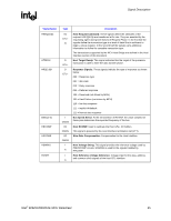
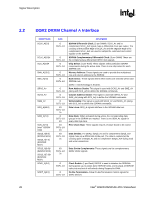
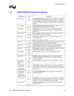
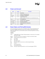
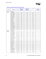
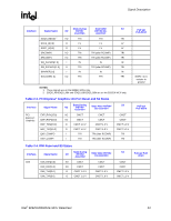
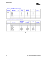
Signal Description R 2.8 2.9 Power and Ground Name VCC VTT VCC_EXP VCCSM VCC2 VCCA_EXPPLL VCCA_HPLL VCCA_SMPLL VSS Voltage 1.5 V 1.2 V 1.5 V 1.8 V 2.5 V 1.5 V 1.5 V 1.5 V 0 V Description Core Power. Processor System Bus Power. PCI Express* and DMI Power. System Memory Power. DDR2: VCCSM = 1.8 V (VCCSM = 1.9 V for DDR2 533 CAS 3-3-3) 2.5 V CMOS Power. PCI Express PLL Analog Power. Host PLL Analog Power. System Memory PLL Analog Power. Ground. Reset States and Pull-up/Pull-downs This section describes the expected states of the MCH I/O buffers during and immediately after the assertion of RSTIN#. This table only refers to the contributions on the interface from the MCH and does not reflect any external influence (such as external pull-up/pull-down resistors or external drivers). Legend: CMCT: DRIVE: TERM: LV: HV: IN: ISO: TRI: PU: PD: STRAP: Common Mode Center Tapped. Differential signals are weakly driven to the common mode central voltage. Strong drive (to normal value supplied by core logic if not otherwise stated) Normal termination devices are turned on Low voltage High voltage Input buffer enabled Isolate input buffer so that it does not oscillate if input left floating Tri-state Weak internal pull-up Weak internal pull-down Strap input sampled during assertion or on the de-asserting edge of RSTIN# 30 Intel® 82925X/82925XE MCH Datasheet
-
 1
1 -
2
-
3
-
4
-
5
-
6
-
7
-
8
-
9
-
10
-
11
-
12
-
13
-
14
-
15
-
16
-
17
-
18
-
19
-
20
-
21
-
22
-
23
-
24
-
 25
25 -
 26
26 -
 27
27 -
 28
28 -
 29
29 -
 30
30 -
 31
31 -
 32
32 -
 33
33 -
 34
34 -
 35
35 -
36
-
37
-
38
-
39
-
40
-
41
-
42
-
43
-
44
-
45
-
46
-
47
-
48
-
49
-
50
-
51
-
52
-
53
-
54
-
55
-
56
-
57
-
58
-
59
-
60
-
61
-
62
-
63
-
64
-
65
-
66
-
67
-
68
-
69
-
70
-
71
-
72
-
73
-
74
-
75
-
76
-
77
-
78
-
79
-
80
-
81
-
82
-
83
-
84
-
85
-
86
-
87
-
88
-
89
-
90
-
91
-
92
-
93
-
94
-
95
-
96
-
97
-
98
-
99
-
100
-
101
-
102
-
103
-
104
-
105
-
106
-
107
-
108
-
109
-
110
-
111
-
112
-
113
-
114
-
115
-
116
-
117
-
118
-
119
-
120
-
121
-
122
-
123
-
124
-
125
-
126
-
127
-
128
-
129
-
130
-
131
-
132
-
133
-
134
-
135
-
136
-
137
-
138
-
139
-
140
-
141
-
142
-
143
-
144
-
145
-
146
-
147
-
148
-
149
-
150
-
151
-
152
-
153
-
154
-
155
-
156
-
157
-
158
-
159
-
160
-
161
-
162
-
163
-
164
-
165
-
166
-
167
-
168
-
169
-
170
-
171
-
172
-
173
-
174
-
175
-
176
-
177
-
178
-
179
-
180
-
181
-
182
-
183
-
184
-
185
-
186
-
187
-
188
-
189
-
190
-
191
-
192
-
193
-
194
-
195
-
196
-
197
-
198
-
199
-
200
-
201
-
202
-
203
-
204
-
205
-
206
-
207
-
208
-
209
-
210
-
211
-
212
-
213
-
214
-
215
-
216
-
217
-
218
-
219
-
220
-
221
-
222
-
223
-
224
-
225
-
226
-
227
-
228
-
229
-
230
-
231
-
232
-
233
-
234
-
235
-
236
-
237
-
238
-
239
-
240
-
241
-
242
 |
 |