Intel 925 Data Sheet - Page 129
PM_CS1-Power Management Control/Status, D1:F0, PCI Device, Address Offset, Default Value, Access, RO
 |
UPC - 683728067724
View all Intel 925 manuals
Add to My Manuals
Save this manual to your list of manuals |
Page 129 highlights
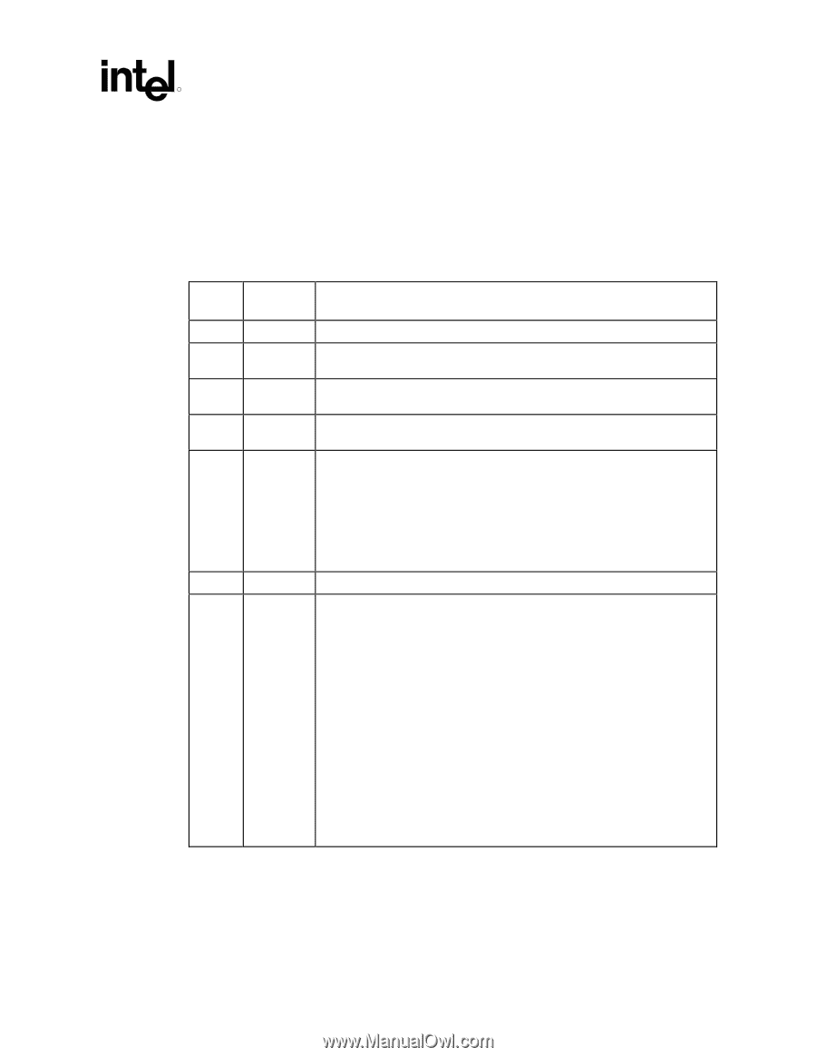
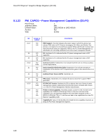
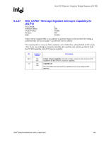
Host-PCI Express* Graphics Bridge Registers (D1:F0) R 8.1.24 PM_CS1-Power Management Control/Status (D1:F0) PCI Device: Address Offset: Default Value: Access: Size: 1 84h 00000000h RO, R/W/S 32 bits Bit 31:16 15 14:13 12:9 8 7:2 1:0 Access & Default RO 0b RO 00b RO 0h R/W/S 0b R/W 00b Description Reserved PME Status: This bit indicates that this device does not support PME# generation from D3cold. Data Scale: This field indicates that this device does not support the power management data register. Data Select: This field indicates that this device does not support the power management data register. PME Enable: This bit indicates that this device does not generate PMEB assertion from any D-state. 0 = PMEB generation not possible from any D State 1 = PMEB generation enabled from any D State The setting of this bit has no effect on hardware. See PM_CAP[15:11] Reserved Power State: This field indicates the current power state of this device and can be used to set the device into a new power state. If software attempts to write an unsupported state to this field, write operation must complete normally on the bus, but the data is discarded and no state change occurs. 00 = D0 01 = D1 (Not supported in this device.) 10 = D2 (Not supported in this device.) 11 = D3 Support of D3cold does not require any special action. While in the D3hot state, this device can only act as the target of PCI configuration transactions (for power management control). This device also cannot generate interrupts or respond to MMR cycles in the D3 state. The device must return to the D0 state to be fully functional. There is no hardware functionality required to support these power states. Intel® 82925X/82925XE MCH Datasheet 129
-
 1
1 -
2
-
3
-
4
-
5
-
6
-
7
-
8
-
9
-
10
-
11
-
12
-
13
-
14
-
15
-
16
-
17
-
18
-
19
-
20
-
21
-
22
-
23
-
24
-
25
-
26
-
27
-
28
-
29
-
30
-
31
-
32
-
33
-
34
-
35
-
36
-
37
-
38
-
39
-
40
-
41
-
42
-
43
-
44
-
45
-
46
-
47
-
48
-
49
-
50
-
51
-
52
-
53
-
54
-
55
-
56
-
57
-
58
-
59
-
60
-
61
-
62
-
63
-
64
-
65
-
66
-
67
-
68
-
69
-
70
-
71
-
72
-
73
-
74
-
75
-
76
-
77
-
78
-
79
-
80
-
81
-
82
-
83
-
84
-
85
-
86
-
87
-
88
-
89
-
90
-
91
-
92
-
93
-
94
-
95
-
96
-
97
-
98
-
99
-
100
-
101
-
102
-
103
-
104
-
105
-
106
-
107
-
108
-
109
-
110
-
111
-
112
-
113
-
114
-
115
-
116
-
117
-
118
-
119
-
120
-
121
-
122
-
123
-
 124
124 -
 125
125 -
 126
126 -
 127
127 -
 128
128 -
 129
129 -
 130
130 -
 131
131 -
 132
132 -
 133
133 -
 134
134 -
135
-
136
-
137
-
138
-
139
-
140
-
141
-
142
-
143
-
144
-
145
-
146
-
147
-
148
-
149
-
150
-
151
-
152
-
153
-
154
-
155
-
156
-
157
-
158
-
159
-
160
-
161
-
162
-
163
-
164
-
165
-
166
-
167
-
168
-
169
-
170
-
171
-
172
-
173
-
174
-
175
-
176
-
177
-
178
-
179
-
180
-
181
-
182
-
183
-
184
-
185
-
186
-
187
-
188
-
189
-
190
-
191
-
192
-
193
-
194
-
195
-
196
-
197
-
198
-
199
-
200
-
201
-
202
-
203
-
204
-
205
-
206
-
207
-
208
-
209
-
210
-
211
-
212
-
213
-
214
-
215
-
216
-
217
-
218
-
219
-
220
-
221
-
222
-
223
-
224
-
225
-
226
-
227
-
228
-
229
-
230
-
231
-
232
-
233
-
234
-
235
-
236
-
237
-
238
-
239
-
240
-
241
-
242
 |
 |